3. TECHNICAL BRIEF
- 18 -
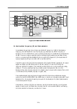
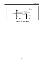
Figure 3-4 SI4205 FREQUENCY SYNTHESIZER PART
The Aero I transceiver integrates two complete PLLs including VCOs, varactors, resonators, loop
filters, reference and VCO dividers, and phase detectors. The RF PLL uses two multiplexed
VCOs. The RF1 VCO is used for receive mode, and the RF2 VCO is used for transmit mode.
The IF PLL is used only during transmit mode. All VCO tuning inductors are also integrated. The
IF and RF output frequencies are set by programming the N-Divider registers, N
RF1
, N
RF2
and
NIF. Programming the N-Divider register for either RF1 or RF2 automatically selects the proper
VCO. The output frequency of each PLL is as follows:
The DIV2 bit in register 31h controls a programmable divider at the XIN pin to allow either a 13
or 26 MHz reference frequency. For receive mode, the RF1 PLL phase detector update rate ( )
should be programmed = 100 kHz for DCS 1800 or PCS 1900 bands, and = 200 kHz for
GSM 850 and E-GSM 900 bands. For transmit mode, the RF2 and IF PLL phase detector
update rates are always =200 kHz.
(3) Frequency Synthesizer
Содержание B2070
Страница 54: ... 53 4 TROUBLE SHOOTING 4 2 TX Trouble TEST POINT 13Mhz OSCILLATOR Mobile SW FEM TRANCEIVER LDO PAM ...
Страница 68: ... 67 4 TROUBLE SHOOTING TEST POINT 4 6 LCD Trouble ...
Страница 72: ... 71 4 TROUBLE SHOOTING TEST POINT 4 8 Speaker Trouble ...
Страница 79: ... 78 4 TROUBLE SHOOTING 4 11 KEY backlight Trouble TEST POINT ...
Страница 96: ...6 Press Start and Pover on the phone using JIG remote Power on Switch 1 5 DOWNLOAD AND CALIBRATION 95 ...
Страница 107: ... 106 8 PCB LAYOUT Figure 8 1 B2070 BOTTOM SIDE PCB LAYOUT ...
Страница 108: ... 107 8 PCB LAYOUT Figure 8 1 B2070 TOP SIDE PCB LAYOUT ...
Страница 109: ... 108 ...
Страница 117: ...10 STAND ALONE TEST 116 Figure 10 2 HW test setting Figure 10 3 Ramping profile ...
Страница 121: ... 120 ...
Страница 123: ... 122 ...

