background image

3: Demonstration Kit 

MatchPort b/g Pro Integration Guide 

25 

Configuration Switch Bank 

Table 3-3. Demo Board JP1 Jumper Configuration 

JP1 pin/Signal  JP1 pin/Signal  Function 

1/CP1 

2/LED12 

Jumper 1-2, CP1 Controls LED12 

3/CP2 

4/LED11 

Jumper 3-4, CP2 Controls LED11 

5/CP3 

6/LED10 

Jumper 5-6, CP3 Controls LED10 

7/CP4 

8/LED9 

Jumper 7-8, CP4 Controls LED9 

9/CP5 

10/LED8 

Jumper 9-10, CP5 Controls LED8 

11/CP6 

12/LED7 

Jumper 11-12, CP6 Controls LED7 

13/CP7 

14/LED6 

Jumper 13-14, CP7 Controls LED6 


Table 3-4. Demo Board JP7 Jumper Configuration for CON1 

JP7 
pin/Signal 

JP7 
pin/Signal 

Function 

1/TXD1 

2/TXA 

Jumper 1-2, Send TXD to RS232/485 transceiver. 

3/RTS1 

4/RTSA 

Jumper 3-4, Send RTS to RS232/485 transceiver. In 485 mode RTS 
controls transmit enable. 

5/CP3 

6/SEL4XXA 

Jumper 5-6, CP3 high selects 485 mode, low 232 mode. Pin at 
transceiver is pulled down to default to 232 mode. 

7/RXD1 

8/RXA 

Jumper 7-8, Receive RXD from RS232/485 transceiver. 

9/CTS1 

10/CTSA 

Jumper 9-10, Receive CTS from RS232 transceiver. 

11/CP4 

12/HDPX4XXA 

Jumper 11-12. In 485 mode, CP4 selects full duplex when low and 
half-duplex when high. Pin at transceiver is pulled down to default to 
full duplex. 

13/CP1 

14/DTRA 

Jumper 13-14, CP1 drives DTR to RS232 transceiver. 

15/CP2 

16/DCDA 

Jumper 15-16, CP2 receives DCD from RS232 transceiver. 

Table 3-5. Demo Board JP8 Jumper Configuration for CON2 

JP7 
pin/Signal 

JP7 
pin/Signal 

Function 

1/TXD2 

2/TXB 

Jumper 1-2, Send TXD to RS232 transceiver. 

3/RTS2 

4/RTSB 

Jumper 3-4, Send RTS to RS232 transceiver.  

5/CP7 

6/SEL4XXB 

Do 

not

 add jumper since only RS232 is supported. Pin at 

transceiver is pulled down to default to 232 mode. 

7/RXD2 

8/RXB 

Jumper 7-8, Receive RXD from RS232 transceiver. 

9/CTS2 

10/CTSB 

Jumper 9-10, Receive CTS from RS232 transceiver. 

11/RESERVED 
on MatchPort 
b/g Pro 

12/HDPX4XXB 

Do 

not

 add jumper since only RS232 is supported. Pin at 

transceiver is pulled down to default to 232 mode. 

13/CP5 

14/DTRB 

Jumper 13-14, CP5 drives DTR to RS232 transceiver. 

15/CP6 

16/DCDB 

Jumper 15-16, CP6 receives DCD from RS232 
transceiver. 

Table 3-6. Demo Board JP8 Jumper Configuration for CON2 

JP7 
pin/Signal 

JP7 
pin/Signal 

Function 

1/TXD2 

2/TXB 

Jumper 1-2, Send TXD to RS232 transceiver. 

3/RTS2 

4/RTSB 

Jumper 3-4, Send RTS to RS232 transceiver.  

5/CP7 

6/SEL4XXB 

Do 

not

 add jumper since only RS232 is supported. Pin at 

transceiver is pulled down to default to 232 mode. 

7/RXD2 

8/RXB 

Jumper 7-8, Receive RXD from RS232 transceiver. 

9/CTS2 

10/CTSB 

Jumper 9-10, Receive CTS from RS232 transceiver. 

11/RESERVED 
on MatchPort 

12/HDPX4XXB 

Do 

not

 add jumper since only RS232 is supported. Pin at 

transceiver is pulled down to default to 232 mode. 

Содержание MatchPort b/g Pro

Страница 1: ...Part Number 900 532 Revision B December 2011 MatchPort b g Pro Integration Guide...

Страница 2: ...protection against radio interference in a residential installation This equipment generates uses and can radiate radio frequency energy and if not installed and used in accordance with this guide ma...

Страница 3: ...ed The required antenna impedance is 50 ohms To reduce potential radio interference to other users the antenna type and its gain should be so chosen that the equivalent isotropically radiated power EI...

Страница 4: ..._______ 13 IO Configurable Pins CPs _______________________________________________ 15 BOOTP_EN __________________________________________________________ 16 BOOTP enable _____________________________...

Страница 5: ...6 Product Label __________________________________________________ 22 Figure 3 1 MatchPort Demo Board Layout______________________________________ 27 Figure 3 2 Demo Board Block Diagram ______________...

Страница 6: ...their product Additional Documentation The following guides are available on the product CD and the Lantronix Web site www lantronix com MatchPort b g Pro User Guide Provides information needed to co...

Страница 7: ...U FL connector for external antenna 802 11i and 802 1X security standards supported Ethernet 10 100 Base TX with auto negotiation and HP auto MDIX On board 100 ohm terminations included External RJ45...

Страница 8: ...2 Description and Specifications MatchPort b g Pro Integration Guide 8 Figure 2 1 MatchPort b g Pro Block Diagram...

Страница 9: ...gurable Pin 7 P1 35 RSVD Reserved Do not connect P1 37 S3 3V I 3 3V Power Input P1 39 GND I Ground PIN NAME Dir Active level FUNCTION P2 2 GND I Ground P2 4 RSVD Reserved Do not connect P2 6 ETX O PHY...

Страница 10: ...d at the RESETIN to filter out transient voltages However it is a good practice to have RESETIN trace on the target board as short as possible to avoid reset occurrences when transient voltages such a...

Страница 11: ...at POR causing undesired operation Wireless LED Connections The W_LINKLED is driven by the Radio Module Active low Open drain 10mA max Recommended connections on the target board are shown below The...

Страница 12: ...cable supplier Figure 2 7 R SMA Antenna Connector Dimensions not to scale Antenna The MatchPort b g Pro has been FCC certified with a 5 dBi gain antenna for wireless 802 11b g It is for applications w...

Страница 13: ...line drivers and DTE style DB9 connectors Table 2 1 RS232 Connections MatchPort b g Pro DCE Connector DTE Connector Signal Logic Description DB9 DB25 Signal DB9 DB25 Signal RXD1 Data In 2 3 RXD1 3 2...

Страница 14: ...2 Description and Specifications MatchPort b g Pro Integration Guide 14 Figure 2 9 Separate RS232 422 Transceivers...

Страница 15: ...ins CPs There are up to seven CPs if no DTR or DCD is used on the serial ports All CPs have internal pull up resistors but the value differs See table CPs can be configured for special functions like...

Страница 16: ...on In case an error occurs during the bootloader operation it will flash the LED The pattern will be pause X long flashes Y short flashes pause X long flashes etc X is the first digit of the error num...

Страница 17: ...ERX Voltage VETH 0 VCC 0 3 Vdc Operating Temperature 40 70 o C Storage Temperature 40 85 o C Table 2 4 Recommended Operating Conditions Parameter Symbol Min Typical Max Units Supply Voltage VCC 3 135...

Страница 18: ...DQPSK CCK OFDM 16QAM 64QAM Security WEP WPA WPA2 802 11i EAP TLS EAP TTLS PEAP LEAP Maximum Receive Level 10 dBm with PER 8 Receiver Sensitivity 69 dBm for 54 Mbps 88 dBm for 11 Mbps 85 dBm for 6 Mbp...

Страница 19: ...uilt in web manager or custom pages in onboard FLASH filesystem Custom storage FLASH filesystem with 2 5 MB capacity Security Password protection locking features Average Power Consumption at 3 3V 0 3...

Страница 20: ...2 Description and Specifications MatchPort b g Pro Integration Guide 20 Figure 2 13 Top View Figure 2 14 Bottom View...

Страница 21: ...nd other signals Set up PCB routing properties on each pair ETX ETX and ERX ERX to achieve 100 ohm impedance For EMI purposes connect the metal housing shield of the RJ45 jack to Power Ground or Earth...

Страница 22: ...Guide 22 Product Information Label The product information label contains important information about your specific unit such as its product ID name bar code part number and MAC address Figure 2 16 Pr...

Страница 23: ...firmware on the MatchPort b g Pro Lantronix offers a MatchPort Plus Development board with a Background Debug Mode BDM connector together with a Software Development Kit SDK Please contact Lantronix f...

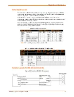
Страница 24: ...ut 7 DCD1_232 Modem Control Input 1 DTR1_232 Modem Control Output 4 GND Ground 5 Table 3 x RS 232 Signals on Serial Port 2 MatchPort Demo PIN FUNCTION DB9 Pin Serial Port 2 CON2 TX2_232 Data Out 3 RX2...

Страница 25: ...transceiver 15 CP2 16 DCDA Jumper 15 16 CP2 receives DCD from RS232 transceiver Table 3 5 Demo Board JP8 Jumper Configuration for CON2 JP7 pin Signal JP7 pin Signal Function 1 TXD2 2 TXB Jumper 1 2 S...

Страница 26: ..._UUT Jumper 1 2 MatchPort module power supply Note Jumper can be replaced with short wire to allow use of a current clamp or 50 milliohm resistor to allow use of voltmeter for current measurements If...

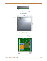
Страница 27: ...3 Demonstration Kit MatchPort b g Pro Integration Guide 27 Demo Board Layout Figure 3 1 MatchPort Demo Board Layout...

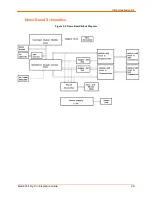
Страница 28: ...3 Demonstration Kit MatchPort b g Pro Integration Guide 28 Demo Board Schematics Figure 3 2 Demo Board Block Diagram...

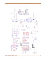
Страница 29: ...3 Demonstration Kit MatchPort b g Pro Integration Guide 29 Figure 3 3 Schematic...

Страница 30: ...3 Demonstration Kit MatchPort b g Pro Integration Guide 30 Figure 3 3 Schematic continued...

Страница 31: ...3 Demonstration Kit MatchPort b g Pro Integration Guide 31 Figure 3 3 Schematic continued...

Страница 32: ...15 Subpart B and C Class B FCC Module Approval FCC Identifier R68MPBGPRO Industry Canada ICES 003 Issue 4 2004 Class B Industry Canada RSS Gen Issue 2 2007 Industry Canada RSS 210 Issue 7 2007 Indust...

Страница 33: ...MatchPort b g Pro Integration Guide 33 B Warranty For details on the Lantronix warranty replacement policy go to our web site at www lantronix com support warranty...

Отзывы: