46
c
HAPTER
3:
Operation
F71/F41 Teslameter
3.6.4 Operation
3.6.4.1 Active Area Location
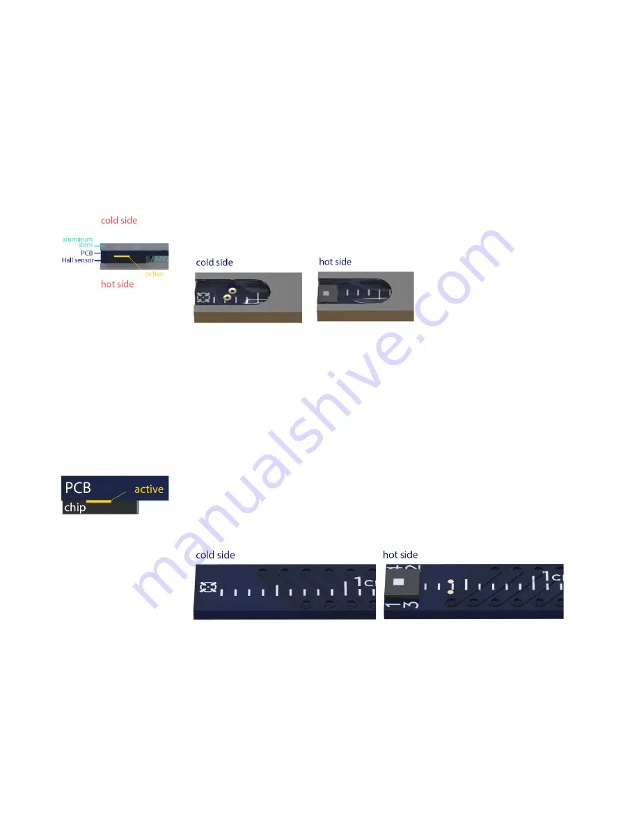
Where possible, active area locations are made visible on the probe. Note that some
probes have active areas that are not centered on the stem axis, meaning that beyond
switching polarity, the magnitude of the field will change if the stem is rotated in a
fixed magnetic field. The side of the stem closest to the stem surface, resulting the
largest field reading possible, is referred to as the “hot” side; the reverse side is
referred to as the “cold” side. This concept is most important when working with
transverse probes, though this should also be considered with 3-axis probes.
3.6.4.1.1 Transverse Standard (TS)
The sensing element is the black chip positioned on one side of the stem, with a white
spot painted on the chip to indicate where the active element is located. On the oppo-
site side of the probe, a target indicator is painted on the PCB to show the active area
when the sensor is facing away from the operator.
The active area of the sensing element is on the surface of the chip where it meets the
stem PCB. This means the “hot” side of the probe contains the Hall effect chip and the
“cold” side contains the target indicator.
3.6.4.1.2 Transverse Flexible-Thin (TF)
This stem follows the same principals of the transverse standard probe, however, the
aluminum stem is removed, completely exposing the stem PCB. Given that this stem
is designed to fit into very thin gaps, it may be difficult to identify the position of the
active area once inside the gap.
A ruler has been added to the stem indicating distance from the active area (not the
tip of the stem).
FIGURE 3-44
Transverse Standard (TS) probe
active area
FIGURE 3-45
Transverse Standard (TS) probe
Left: cold side; Right: hot side
FIGURE 3-46
Transverse Flexible-Thin (TF)
probe active area
FIGURE 3-47
Transverse Flexible-Thin (TF) probe
Left: cold side; Right: hot side


