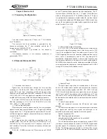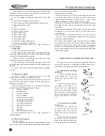
Figure 3.9 Transmitter Audio Circuits
R512, R513, R514 are the amplifier current checker; IC10A the
sample amplifier of the amplification current. IC10B is the power
comparison amplifier.
If the transmitter output power is too high, the amplifier current
will increase, IC10A output will mount, IC10B output voltage
decrease, the offset voltage added to Q67 and Q68 will decrease,
and then the transmitter output power will decrease. Vice versa,
such can ensure steady transmitter output power in different
working circumstances.
MCU changes the voltage input to IC10B to set the power.
Transmitter Audio Signal Processing
IC14, IC12 and the peripherals components compose the
transmitter audio processing circuit. The audio signals from MIC are
amplified to be sent to MCU after the demodulation (VOX signal);
simultaneously they are amplified after preemphasis, amplitude limit
and filtration in the C12 where they have been sent there through
the ACC circuit and finally sent to VCO modulation together with
CTCSS/DCS for modulation.
J2 is the external MIC socket, when the external MIC is used,
the internal MIC will be off automatically while the internal PTT will
remain activated.
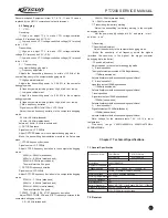
Figure 3.10 Frequency Synthesizer
The radio adopts Phase Locked Loop (PLL) frequency
synthesizer.
The frequency synthesizer consists of standard oscillator,
voltage controlled oscillator (VCO), programmable frequency
demultiplier, phase comparator, and low pass filter.
IC9 (ADF4111) is PLL integrated circuit, including
programmable reference frequency demultiplier, programmable
frequency demultiplier, phase comparator, and charge pump.
R334, C464, R333, R311, C448, C484 and R336 construct the
low pass filter.
The standard frequency is supplied by X4 (TCXO, 12.8MHz).
The standard frequency from TCXO (Temperature Control
Transistor Oscillator) is demultiplied by the programmable reference
frequency demultiplier at IC9 to acquire 6kHz or 6.5kHz reference
frequency (controlled by MCU according to the preset channel
frequency).
The oscillation frequency from VCO is sent to IC1, and
demultiplied by programmable frequency demultiplier and
compared with reference frequency to acquire the error signals.
Then pass the low pass filter and are sent to VCO to change VCO
oscillation frequency to the preset value, and then VCO is locked.
N=F
/F
VCO
R
N: Frequency demultiplication times
F
: VCO oscillation frequency
VCO
F : Reference frequency
R
Check Loss of Lock: When PLL is in loss of lock, IC pin14
sends out low level signals to MCU, which controls the transmitter
not to transmit and initiate warning tone.
3.5 Voice Prompt Circuit:
The radio features voice prompt, which is very useful at night or
in the environment of dim light.
The internal memory IC of MCU is provided with voices like
channel indication, etc., each time switch a channel, the speaker
will prompt the current channel number by voice prompt.
3.6 Power Supply:
The radio is equipped with 7.4V, 1700mAh li-polymer battery,
transmitter power amplifier circuit (Q67, Q68), receiver audio power
amplifier (Q92) directly adopt the power supplied by the battery and
other circuits adopt the regulated 5V to supply power.
U13: 5V low voltage difference, micro-power regulator, together
with U12 to supply 5V power with high current.
Q76: T5V switch, controlled by MCU.
T5V: Supply power for the Transmitter front terminal
Q85: R5V switch, controlled by MCU.
R5V: Supplies power for the receiver RF amplification, mixing,
IF processing, audio signal processing.
Q83: C5V switch, controlled by MCU.
C5V: The 5V power controlled by power saving supplies power
for the frequency synthesizer.
3.4 Frequency Synthesizer
to decode CTCSS/DCS more precisely.
3.3 Transmitter (TX)
Transmitter Power Amplifier
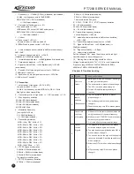
Figure 3.7 Amplifier and antenna switch diagram
The modulated RF signals from VCO are amplified at Q60, Q66,
Q67 and then are sent to Q68 for power amplification. Q68 output
power: 4.5W.
The Q67, Q68 grid offset is controlled by APC circuit. Changing
the grid bias can control the transmitter output power conveniently.
APC (Auto Power Control)
Figure 3.8 APC Circuits
PT7200 SERVICE MANUAL
3
Содержание PT7200-01
Страница 1: ...PROFESSIONAL TWO WAY RADIO PT7200 V071215 FM PORTABLE RADIO SERVICE MANUAL ...
Страница 29: ...Figure 1 PT7200 Top Board Position Mark Diagram 136 174 ...
Страница 30: ......
Страница 31: ...Figure 1 PT7200 Top Board Position Mark Diagram 400 470 ...
Страница 32: ......
Страница 35: ...Figure 7 Schematic Circuit Pane Diagram PT7200 SERVICE MANUAL 26 33 ...


