


PT568 Service Manual
9
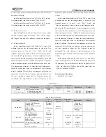
Figure 4.1
C.
Turn the computer power ON.
D.
Turn the radio power ON.
E.
Run the KSP568 programming software by double
clicking on its executive program.
F.
Click “Program” in the main menu of KSP568, and click
“Read from radio” in the pull-down menu to read
parameters of the radio to the computer; click “Write to
radio” in the pull-down menu to write parameters in the
computer to the radio.
G.
The following parameters can be set by using KSP568
according to requirements of the user:
Radio Information:
Radio Model (model/frequency range), Serial Number,
Embedded Information, MCU Version, Hardware Version, etc.
Radio Parameters:
1)
Key Assignment: P1, P2, P3 can be set as long/short key and
the hold time can be defined.
No.
Function
Description
0 None
No function is assigned.
1
Voice
Annunciation
Press the preprogrammed “Voice Annunciation” button to
change the language and mode of voice annunciation.
Meanwhile, the current channel number can be heard.
2 Talk
Around
When the preprogrammed “Talk Around” button is
pressed, the next transmission will be at the same
frequency as at which it is received.
3 Lone
Worker
Press the preprogrammed “Lone Worker” button to
start/stop lone working.
4
Emergency
Alarm
Press the preprogrammed “Emergency Alarm” button to
make warning tone according to the setting of the
programming software or send your ID or background
sound to your partner or the system. (This function can
only be assigned to the TOP KEY)
5
Emergency
Alarm Off
Press the preprogrammed “Emergency Alarm Off” button
to quit the Emergency Alarm Mode. (This function can
only be assigned to the TOP KEY, and should be used
together with Emergency Alarm function)
6 Scan
Press the preprogrammed “Scan” button to start/stop
scanning.
7
Nuisance
Delete(tempo
rary)
If the radio stays at a noise channel while scanning, press
the preprogrammed “Nuisance Delete” button to delete the
nuisance channel temporarily.
8
High/Low
Power Switch
Press the preprogrammed “High/Low Power Switch”
button to switch between high and low transmitting power
of the radio.
9
Momentary
Monitor
Press and hold the preprogrammed “Momentary Monitor”
button to disable CTCSS, DCS signalling, and release the
button to resume normal operation.
10 Monitor
Press the preprogrammed “Monitor” button to disable
CTCSS, DCS signalling, and you can receive signals that
cannot be heard under normal operation. Press it again to
resume normal operation.
11
Momentary
Squelch Off
Press and hold the preprogrammed “Momentary Squelch
Off” button to open squelch; release it to resume normal
operation
12 Squelch Off
Press the preprogrammed “Squelch Off” button to open
squelch. Press it again to resume normal operation.
13
Lone Worker
Reset
Press the preprogrammed “Lone Worker Reset” button
while the radio is in Lone Worker Mode to reset the lone
worker timer, and the timer starts again.
14 FCS
Press to start free channel scanning (FCS).
2) Optional Functions
1. Wired Clone enable
2. All Low Power Switch
3. Firmware Programming Mode enable
4. Beep Tone
5. All Low Power
6. Voice Annunciation Setting
7. Battery Save
8. TOT
9. TOT Reset Time
10. TOT Pre-alert
11. TOT Rekey Time
12. Squelch Level Selection
3) Embedded Information
1. Password of Read Radio
2. Password of Write Radio
3. Embedded Information Setting
4) Scan
Scan function setting: Priority Channel selection, Revert
Channel selection, Tx Dwell Time, Dropout Delay Time,
Lookback Time.
FCS function setting: Automatic Tx Time, Automatic Rx Time,
FCS Resume Time, Scanning Times.
5) Emergency Setting
Press the preprogrammed “Emergency Alarm” button (the
hold time should be longer than the debounce time of the
emergency alarm switch) to enter Emergency Alarm Mode. The
radio can make warning tone according to the setting of the
programming software, or send the background sound to your
partner or the system.
Press the preprogrammed “Emergency Alarm Off” button to
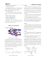
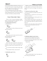
Computer
(RS232 serial port)
Programming
cable
Radio
(Earphone/Program
ming interface)
Содержание PT568-01
Страница 26: ......
Страница 27: ......
Страница 28: ...PT568 Service Manual 28 Figure 5 PT568 Top Layer Position Value Diagram ...
Страница 29: ...PT568 Service Manual 29 Figure 6 PT568 Bottom Layer Position Value Diagram ...


