TKR-740
34
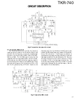
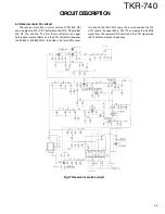
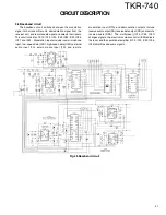
4.3 Wide IF circuit
The w ide IF circuit consists of tw o-pole M CF XF1, four-
pole M CF XF3, IF amplifier Q24, IF amplifier Q31, FM detector
IC IC8, crystal oscillator X2, ceramic filter CF2, CF4. The
unw anted components of the signal are removed by tw o-pole
M CF XF1 and four-pole M CF XF3 and the resulting signal is
amplified by IF amplifiers Q24 and Q31. The second IF signal
(450 kHz) is produced by FM detector IC IC8. Unw anted
components of the second IF signal are removed by ceramic
filter CF2, CF4, and the resulting signal is amplified by the
built-in IF amplifier and FM -detected by the quadrature
detection circuit to generate a baseband signal. This signal is
output from pin 15. It then passes through analog switch IC21,
invert amplifier IC15 (A/2) and AF amplifier IC12 (A/2) and goes
to the Y1 input of multiplexer IC and the V1 input of electronic
volume control IC9.
The level of the signal that enters V1 of the electronic
volume control IC is adjusted, the signal passes through AF
sw itch Q35, goes to IC8 noise filter input (pin 17), and high-
frequency components are selected by an HPF consisting of
an external RC netw ork. The signal is noise-detected and the
compared noise squelch signal (N-DET) is fed to DC sw itch
Q36. The signal strength analog voltage (RSSI) from the tw o
second IF amplifiers in IC8 is compared w ith the reference
voltage set by electronic volume control V3 by the internal
RSSI comparator, and the RSSI squelch signal (C-DET) is output
from pin 20 of IC8. C-DET enters DC switch Q37 and is ANDed
w ith the N-DET by DC sw itch Q38 and output as a squelch
signal (SC).
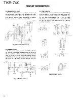
Fig.16 Wide IF circuit
CIRCUIT DESCRIPTION
Содержание TKR-740
Страница 97: ...TKR 740 TKR 740 BLOCKDIAGRAM 121 122 ...
Страница 99: ...TKR 740 TKR 740 INTERCONNECTION DIAGRAM 125 126 ...
Страница 101: ...MEMO 129 ...


