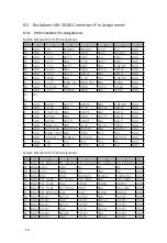
background image

19

Pin  Z 

8  GND  AD[56] 

AD[55] 

AD[54] 

GND 

AD[53] 

GND 

7  GND  AD[59] 

GND 

V(I/O) 

AD[58] 

AD[57] 

GND 

6  GND  AD[63] 

AD[62] 

AD[61] 

GND 

AD[60] 

GND 

5  GND 

C/BE[5]# 

GND 

V(I/O) 

C/BE[4]# 

PAR64 

GND 

4  GND 

V(I/O) 

PXI_BRSVB4  C/BE[7]# 

GND 

C/BE[6]# 

GND 

3  GND  CLK4 

GND 

GNT3# 

REQ4# 

GNT4# 

GND 

2  GND  CLK2 

CLK3 

GND (SYS#)  GNT2# 

REQ3# 

GND 

1  GND  CLK1 

GND 

REQ1# 

GNT1# 

REQ2# 

GND 

Star Trigger Slot (Slot #2) P1 Pin Assignment 
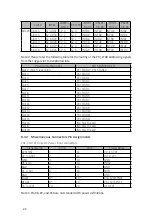
Pin 

25 

GND  +5V 

REQ64# 

ENUM# 

+3.3V 

+5V 

GND 

24 

GND  AD[1] 

+5V 

V(I/O) 

AD[0] 

ACK64# 

GND 

23 

GND  +3.3V 

AD[4] 

AD[3] 

+5V 

AD[2] 

GND 

22 

GND  AD[7] 

GND 

+3.3V 

AD[6] 

AD[5] 

GND 

21 

GND  +3.3V 

AD[9] 

AD[8] 

M66EN 

C/BE[0]# 

GND 

20 

GND  AD[12] 

GND 

V(I/O) 

AD[11] 

AD[10] 

GND 

19 

GND  +3.3V 

AD[15] 

AD[14] 

GND 

AD[13] 

GND 

18 

GND 

SERR# 

GND 

+3.3V 

PAR 

C/BE[1]# 

GND 

17 

GND  +3.3V 

IPMB_SCL  IPMB_SDA 

GND 

PERR# 

GND 

16 

GND 

DEVSEL# 

GND 

V(I/O) 

STOP# 

LOCK# 

GND 

15 

GND  +3.3V 

FRAME# 

IRDY# 

GND 

TRDY# 

GND 

12-
14 

Key 

11 

GND  AD[18] 

AD[17] 

AD[16] 

GND 

C/BE[2]# 

GND 

10 

GND  AD[21] 

GND 

+3.3V 

AD[20] 

AD[19] 

GND 

GND 

C/BE[3]# 

IDSEL (1) 

AD[23] 

GND 

AD[22] 

GND 

GND  AD[26] 

GND 

V(I/O) 

AD[25] 

AD[24] 

GND 

GND  AD[30] 

AD[29] 

AD[28] 

GND 

AD[27] 

GND 

GND 

REQ# (1) 

GND 

+3.3V 

CLK (1) 

AD[31] 

GND 

GND 

BRSVP1A5  BRSVP1B5  PCIRST# 

GND 

GNT# (1) 

GND 

GND 

IPMB_PWR 

GND 

V(I/O) 

INTP 

INTS 

GND 

GND 

INTA# (1)  INTB# (1) 

INTC# (1) 

+5V 

INTD# (1) 

GND 

GND  TCK 

+5V 

TMS 

TDO 

TDI 

GND 

GND  +5V 

-12V 

TRST# 

+12V 

+5V 

GND 

Star Trigger Slot (Slot #2) P2 Pin Assignment 
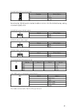
Pin  Z 

22  GND 

PXI_BRSVA22  PXI_BRSVB22  PXI_BRSVC22  PXI_BRSVD22  PXI_BRSVE22 

GND 

21  GND 

PXI_LBR0 

GND 

PXI_LBR1 

PXI_LBR2 

PXI_LBR3 

GND 

20  GND 

PXI_LBR4 

PXI_LBR5 

PXI_STAR0 (2) 

GND 

PXI_STAR1 (2) 

GND 

19  GND 

PXI_STAR2 (2) 

GND 

PXI_STAR3 (2) PXI_STAR4   PXI_STAR5  

GND 

18  GND 

PXI_TRIG3 

PXI_TRIG4  PXI_TRIG5 

GND 

PXI_TRIG6 

GND 

17  GND 

PXI_TRIG2 

GND 

N/C 

PXI_CLK10_IN  PXI_CLK10 

GND 

16  GND 

PXI_TRIG1 

PXI_TRIG0  N/C 

GND 

PXI_TRIG7 

GND 

Содержание PXI-62700

Страница 1: ...PXI 62700 3U 18 Slot PXI Chassis and Accessories User s Manual Manual Revision 1 00 Revision Date Jul 15 2016...

Страница 2: ...equire any service or assistance SHANGHAI JYTEK Co Ltd Web site http www jytek com Address 201203 300 Fang Chun Rd Zhangjiang Hi Tech Park Pudong New Area Shanghai 201203 China Tel 86 21 5047 5899 Fax...

Страница 3: ...ts 6 3 5 Local Bus 6 3 6 Trigger Bus 6 3 7 System Reference Clock 9 4 Troubleshooting and Preventative Maintenance 10 4 1 Troubleshooting the PXI 62700 10 4 2 Cleaning 10 4 2 1 Interior Cleaning 10 4...

Страница 4: ...III Warranty Policy 26...

Страница 5: ...IV List of Tables Table 4 1 Troubleshooting 10...

Страница 6: ...the PXI 62700 chassis 2 Figure 1 2 Rear View of the PXI 62700 chassis 3 Figure 3 1 PXI Local Bus and Star Trigger Routing 8 Figure A 1 PXI 62700 Dimensions 14 Figure B 1 cBX 3018L front view Drawing 1...

Страница 7: ...R Mean Time To Repair 1 1 Unpacking Checklist Check the shipping carton for any damages If the shipping carton and contents are damaged notify the dealer for a replacement Retain the shipping carton a...

Страница 8: ...Two PXI to PXI bridges Figure 1 1 1 2 show some of the feature and components of the PXI 62700 chassis Figure 1 1 shows the front view of the PXI 62700 Figure 12 shows the rear view of the PXI 62700 F...

Страница 9: ...dard backplanes we provide more options for OEM customers as long as the request backplane is PXI or 3U CompactPCI form factor compliant with 21 slot width limitation For example application may requi...

Страница 10: ...r injector handle to fully inject the card into the chassis Secure the screws on the module s front panel Step 4 Install peripheral modules if any Step 5 Press the power switch on the front panel to p...

Страница 11: ...is power RST When the alarm buzzer beeps and the power LED extinguishes you can push power RST button to stop beeping and refer to Chapter 4 5 to hot swap the power supply unit 2 4 Grounding on the M...

Страница 12: ...allow the controller to expand to the left to prevent the controller from using up peripheral slots 3 3 Star Trigger Slot The Star Trigger ST slot is Slot 2 This slot has a dedicated trigger line bet...

Страница 13: ...ferent PXI peripheral modules or use one module to control carefully timed sequences of operations performed on other modules in the system Modules can pass triggers to one another through trigger bus...

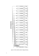
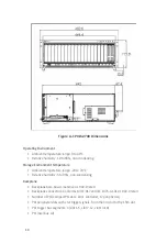
Страница 14: ...8 Figure 3 1 PXI Local Bus and Star Trigger Routing...

Страница 15: ...heral slot Users can use this common reference clock signal to synchronize multiple modules in a measurement or control system or drive PXI_CLK10 from an external source through the PXI_CLK10_IN pin o...

Страница 16: ...the fan hot swap replacement The Power Buzzer is beeping Check if both power supplies have power cord on it If either one of the power supply failed please refer to Chapter 4 5 for the power supply ho...

Страница 17: ...of fans 3 Pull out the defective fan 4 Replace with a new fan 5 Cover back the fans panel cover 4 5 Power Supply Unit Hot Swap Replacement For the PXI 62700 chassis there are four Green LED indicator...

Страница 18: ...ble power 460 W 460 W Output characteristics per module VDC Minimum Maximum Ripple and Noise Max Load Regulation Line Regulation 5 V 5 0 A 40 A 60 mA 5 1 12 V 2 5 A 27 A 100 mA 5 1 5 V 0 A 0 8 A 100 m...

Страница 19: ...ormal condition Flashes if alarm occurs Alarm Buzzer Beep if any alarm occurs Alarm RST button Reset the alarm monitor system Cooling Fans Front access hot swappable fan trays Five 31CFM fans trays at...

Страница 20: ...o 70 C Relative humidity 5 to 95 non condensing Backplane Backplane bare board material UL 94V 0 rated Backplane connectors Conforms to IEC 917 and IEC 1076 4 101 UL 94V 0 rated Number of PXI CompactP...

Страница 21: ...and Vibration Shock 15G peak to peak 11ms duration non operation Random Vibration Operating 5 to 500Hz 0 5GRMS each axis Non operating 5 to 500Hz 1 88GRMS each axis Safety and EMC EMI Compliance Safet...

Страница 22: ...f the backplanes and Mechanical Drawing 1 2 3 4 5 6 9 sys 3 4 5 7 6 8 1 2 8 7 1 0 1 1 1 2 1 7 1 3 1 6 1 5 1 4 9 11 12 13 14 15 16 17 18 10 Figure B 1 cBX 3018L front view Drawing R 1 7 6 5 4 3 2 sys 1...

Страница 23: ...ridge Board Third PCI Bus Slot 13 Third PCI Bus Slot 14 Third PCI Bus Slot 15 Third PCI Bus Slot 16 Third PCI Bus Slot 17 Third PCI Bus Slot 18 64 bit PCI 64 bit PCI 64 bit PCI PXI Trigger bus Group 1...

Страница 24: ...GND 7 GND AD 30 AD 29 AD 28 GND AD 27 GND 6 GND REQ 1 GND 3 3V CLK 1 AD 31 GND 5 GND BRSVP1A5 BRSVP1B5 PCIRST GND GNT 1 GND 4 GND IPMB_PWR GND V I O INTP INTS GND 3 GND INTA 1 INTB 1 INTC 1 5V INTD 1...

Страница 25: ...V I O STOP LOCK GND 15 GND 3 3V FRAME IRDY GND TRDY GND 12 14 Key 11 GND AD 18 AD 17 AD 16 GND C BE 2 GND 10 GND AD 21 GND 3 3V AD 20 AD 19 GND 9 GND C BE 3 IDSEL 1 AD 23 GND AD 22 GND 8 GND AD 26 GN...

Страница 26: ...al Slot Slot 3 6 P1 Pin Assignment Pin Z A B C D E F 25 GND 5V REQ64 ENUM 3 3V 5V GND 24 GND AD 1 5V V I O AD 0 ACK64 GND 23 GND 3 3V AD 4 AD 3 5V AD 2 GND 22 GND AD 7 GND 3 3V AD 6 AD 5 GND 21 GND 3...

Страница 27: ...GND 5 GND C BE 5 GND V I O C BE 4 PAR64 GND 4 GND V I O PXI_BRSVB4 C BE 7 GND C BE 6 GND 3 GND PXI_LBR7 GND PXI_LBR8 PXI_LBR9 PXI_LBR10 GND 2 GND PXI_LBR11 PXI_LBR12 N C SYS PXI_LBL7 PXI_LBL8 GND 1 GN...

Страница 28: ...XI_STAR P2 D17 Slot 2 Star Trigger Slot PXI_STAR0 PXI_STAR12 Slot 3 PXI_STAR0 Slot 4 PXI_STAR1 Slot 5 PXI_STAR2 Slot 6 PXI_STAR3 Slot 7 PXI_STAR4 Slot 8 PXI_STAR5 Slot 9 PXI_STAR6 Slot 10 PXI_STAR7 Sl...

Страница 29: ...t signal J6 Pin Signal Name 1 INH 2 GND J8 RST System reset signal J8 Pin Signal Name 1 RST 2 GND J9 FAL Power supply fail input J9 Pin Signal Name 1 FAL 2 GND J5 Connector for LED power status J5 Nam...

Страница 30: ...24 JP1 10MHz Reference Clock Pin Name 1 2 default Internal 10MHz system clock PXI_CLK10 2 3 External clock through the PXI_CLK10_IN on star trigger slot...

Страница 31: ...transient overvoltage 8 Make sure the voltage of the power source when connect the equipment to the power outlet 9 All cautions and warnings on the equipment should be noted 10 Please keep this equipm...

Страница 32: ...rranty will not cover repair costs due to Damage caused by not following instructions Damage caused by carelessness on the users part during product transportation Damage caused by fire earthquakes fl...

Отзывы: