background image

Appendix B: SE7500CW2Errata documentation 
 

SE7500CW2 Server Board Technical Product Specification 

CXII 


Revision 1.40 


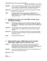
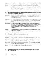
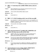
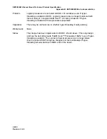
12.  Errata 

1. 

Intel® Xeon processors 2.6 GHz and 2.8 GHz C1  

stepping 

not supported in BIOS 1.14. 

Problem


The SE7500CW2 BIOS 1.14 does not support Intel® Xeon processors running 
at 2.6 Ghz, and 2.8 GHz. 

Implication


Intel® Xeon processors running at 2.6GHz and 2.8GHz won’t boot with the 
currently supported production BIOS 1.14.  In other words, this BIOS doesn’t 
support the C1 stepping that is required by these processors. 

Workaround


None. 

Status


These processor speeds are now supported with BIOS 1.16 and above. Please 
check 

http://support.intel.com

 download details.  Also available on PBA # -505 

and above. 

2. 

Intel® LANDesk Client Manger (LDCM) 6.3 reports different 
processor speeds after a rebooting Windows* 2000 

Problem


Intel® Xeon processor speeds change in the LDCM 6.3 after a reboot.   

Implication


The speed that LDCM reports may be incorrect, and change after a reboot. 
Also, the speed may be slightly slower or faster than actual processor speed. 

Workaround


Use the processor speed listed in BIOS <F2> setup under the “System – CPU” 
sub-menu. 

Status


Intel is investigating the possiblity of fixing this erratum.  

3. 

My SE7500CW2 system won’t boot to DOS with an Adaptec* 
card installed. 

Problem


  SE7500CW2 system boots to the Adaptec SMOR utility instead of booting into 
DOS 

Содержание SE7500CW2

Страница 1: ...SE7500CW2 Server Board Technical Product Specification Intel Document Number C19122 001 Revision 1 40 February 2003 Enterprise Platforms and Services Marketing ...

Страница 2: ...nd grammatical updates from review comments 9 9 2002 1 10 Updated BIOS menus updated BIOS crisis recovery added BIOS Beep codes and MTBF testing results 12 2 2002 1 20 Added Section 9 3 3 on ICH3 power cycling 1 24 2003 1 30 Re added updates BIOS crisis recovery Beep codes MTBF additionally power cycling issues and Specification Update material as Appendix B 2 10 2003 1 40 Updated power cycling pr...

Страница 3: ... any patent copyright or other intellectual property right Intel products are not intended for use in medical life saving or life sustaining applications Intel may make changes to specifications and product descriptions at any time without notice Designers must not rely on the absence or characteristics of any features or instructions marked reserved or undefined Intel reserves these for future de...

Страница 4: ...1 MCH Memory Architecture Overview 11 3 2 2 MCH North Bridge 12 3 2 3 P64H2 12 3 2 4 ICH3 S 13 3 3 Super I O 15 3 3 1 Serial Ports 15 3 3 2 BIOS Flash 16 4 Included PCI Devices 17 4 1 ATA 100 RAID 17 4 2 Video Controller 18 4 3 Network Interface Controller NIC 20 4 4 Optional SCSI Card 20 4 5 Interrupt Routing 21 4 5 1 Legacy Interrupt Routing 21 4 5 2 APIC Interrupt Routing 22 4 5 3 Serialized IR...

Страница 5: ...vanced Configuration and Power Interface ACPI 38 6 3 2 Wake Events 39 6 3 3 Wired For Management WFM 41 6 3 4 Console Redirection 42 6 3 5 Serial Ports 44 6 3 6 System Management BIOS SMBIOS 45 6 3 7 Windows Compatibility 46 6 4 BIOS Serviceability Features 47 6 4 1 Flash Update Utility 48 6 5 BIOS and BIOS Setup 50 6 5 1 BIOS Setup Utility 50 6 5 2 Entering the BIOS Setup Utility 51 6 5 3 Keyboar...

Страница 6: ...8 5 System Management Headers 87 8 5 1 I2 C Header 87 8 6 PCI Slot Connector 87 8 7 Front Panel Connectors 89 8 8 VGA Connector 89 8 9 NIC Connectors 90 8 10 ATA Connectors 90 8 11 USB Connector 91 8 12 Floppy Connector 92 8 13 Serial Port Connectors 93 8 14 Keyboard and Mouse Connector 94 8 15 Miscellaneous Headers and Jumpers 94 8 15 1 Fan Headers 94 8 15 2 System Recovery and Update Jumpers 95 ...

Страница 7: ...netic Compatibility Notices 104 10 2 1 Europe CE Declaration of Conformity 104 10 2 2 Australian Communications Authority ACA C Tick Declaration of Conformity 104 10 2 3 Ministry of Economic Development New Zealand Declaration of Conformity 104 10 2 4 BSMI Taiwan 104 10 3 Replacing the Back Up Battery 105 11 Mechanical Spefications 106 11 1 Mechanical Specifications 106 Appendix A SE7500CW2 Integr...

Страница 8: ...on 8 Figure 4 ATA 100 RAID Level 18 Figure 5 SE7500CW2 Interrupt Routing Diagram ICH3 S Internal 24 Figure 6 SE7500CW2 Interrupt Routing Diagram 25 Figure 7 SE7500CW2 PCI Interrupt Mapping Diagram 26 Figure 8 Intel Server Board SE7500CW2 hardware monitoring 28 Figure 9 SE7500CW2 Configuration Jumpers J106 95 Figure 10 Output Voltage Timing 100 Figure 11 Turn on off Timing 101 Figure 12 SE7500CW2 S...

Страница 9: ...ey Mappings 43 Table 12 ASCII Key Mappings 43 Table 13 SMBIOS Header Structure 45 Table 14 Setup Utility Screen 51 Table 15 Keyboard Commands 51 Table 16 Menu Selection Bar 53 Table 17 Main Menu lists options available It allocates resources for hardware parts 53 Table 18 Primary Secondary Master Slave Submenu 54 Table 19 Advanced Menu 55 Table 20 I O Device Configuration Submenu 57 Table 21 On Bo...

Страница 10: ...MHz PCI Slot Pin out 87 Table 49 P64 B P64 C 3 3V 64 bit 100MHz 133MHz PCI X Slot Pin out 88 Table 50 Front Panel 34 Pin Header Pin out J3 89 Table 51 VGA Connector Pin out J42 90 Table 52 RJ 45 Connector Pin outs J47 90 Table 53 ATA 100 40 pin Connectors Pin out J4 J5 J6 J7 91 Table 54 USB Connectors Pin out J43 91 Table 55 Optional USB Connection Header Pin out J11 91 Table 56 Legacy 34 pin Flop...

Страница 11: ...00CW2 Server Board Technical Product Specification List of Tables xi Revision 1 40 Table 67 Turn On Off Timing 101 Table 68 Transient Load Requirements 102 Table 69 Server Board Connector Specifications 107 ...

Страница 12: ...List of Tables SE7500CW2 Server Board Technical Product Specification xii Revision 1 40 This Page Intentionally Left Blank ...

Страница 13: ...d Overview Chapter 3 Functional Architecture Chapter 4 Included PCI Devices Chapter 5 Hardware Monitoring Chapter 6 System BIOS Chapter 7 Error Handling and Reporting Chapter 8 SE7500CW2 Connectors and Jumper Blocks Chapter 9 General Specifications Chapter 10 Product Regulatory Compliance Chapter 11 Mechanical Specifications 1 1 Audience This document for technical personnel who want a technical o...

Страница 14: ...8 MB of SDRAM Two Intel 10 100 82550PM Fast Ethernet Controllers ATA 100 RAID controller Promise Technology PDC20267 Two PCI slots capable of supporting full length PCI add in cards Segment B PCI X 64 bit 66MHz 3 3 V P64 B with the following configuration Two PCI slots capable of supporting full length PCI add in cards Segment C PCI X 64 bit 133 MHz 3 3 V P64 C with the following device One PCI sl...

Страница 15: ...TA 100 compatible devices Support for up to four system fans and two processor fans SSI compliant connectors for SSI interface support front panel and power connectors The figure below shows the functional blocks of the server board and the plug in modules that it supports Figure 1 SE7500CW2 Server Board Block Diagram 4GB DDR200 or DDR266 memory ...

Страница 16: ...upport The Intel Server Board SE7500CW2supports one or two Intel Xeon processors in the Socket 604 FCPGA2 package When two processors are installed all processors must be of identical revision core voltage and bus core speed When only one processor is installed it should be in the socket labeled CPU1 and the other socket must be empty The support circuitry on the server board consists of the follo...

Страница 17: ... the PMC will not turn on the VRD and a beep code is generated 3 1 1 2 Reset Configuration Logic The BIOS determines the processor stepping cache size etc through the CPUID instruction The requirements are as follows All processors in the system must operate at the same frequency have the same cache sizes and same VID No mixing of product families is supported Processors run at a fixed speed and c...

Страница 18: ...nd chip kill support with DIMMS built on x4 technology Memory can be implemented with either single sided one row or double sided two row DIMMs The figure below provides a block diagram of the memory sub system implemented on the Intel Server Board SE7500CW2 Figure 2 Memory Sub system Block Diagram 1 As of the writing of this document testing with 2GB DIMM modules was not complete and therefore no...

Страница 19: ...DIMMs is 144 bit wide This requires that two DIMMs be populated per bank in order for the system to operate At least one bank has to be populated in order for the system to boot If additional banks have less than two DIMMs the memory for that bank s will not be available to the system There are two banks of DIMMs labeled 1 and 2 Bank 1 contains DIMM locations 1A and 1B and bank 2 contains 2A and 2...

Страница 20: ...face SSTL2 Two DIMMs must be populated in a bank for a 144 bit wide memory data path Any or all memory banks may be populated Table 2 Memory Bank Labels Memory DIMM Bank J39 DIMM 1B J40 DIMM 1A 1 J37 DIMM 2B J38 DIMM 2A 2 Figure 3 Memory Bank Label Definition Bank 2 Bank 1 J37 J38 J39 J40 2B 1B 2A 1A ...

Страница 21: ...SE7500CW2 Server Board Technical Product Specification Functional Architecture 9 Revision 1 40 ...

Страница 22: ...he appropriate controls to control data transfer to and from memory P64H2 PCI X 64bit Hub 2 0 I O Bridge The P64H2 provides the interface for two 64 bit 133 MHz Rev 2 2 compliant PCI X buses implemented on Intel Server Board SE7500CW2 as one bus with one 64 bit 133MHz slot and one bus with two 64 bit 100MHz slots The P64H2 is both master and target on both PCI X buses ICH3 S IO Control Hub South B...

Страница 23: ...ports 64Mb 128Mb 256Mb 512Mb DRAM densities The DDR DIMM interface supports memory scrubbing single bit error correction and multiple bit error detection and chip kill with x4 DIMMs 3 2 1 1 DDR Configurations The DDR interface supports up to 4GB1 of main memory and supports single and double density DIMMs The DDR can be any industry standard DDR The following table shows the DDR DIMM supported Tab...

Страница 24: ...formance main memory subsystem An HI 2 0 bus interface that provides a high performance data flow path between the host bus and the I O subsystem A HI 1 5 bus which provides an interface to the ICH3 S South Bridge Other features provided by the MCH include the following Full support of ECC on the processor bus Full support of chipkill on the memory interface with x4 DIMMs Twelve deep in order queu...

Страница 25: ...I slots on the riser however actual number of slots and slot speeds will be determined by the signal integrity of the riser card used BIOS is responsible for setting the bus speed of P64 C The bus speed will always be set up to run at the speed of the slowest card installed 3 2 4 ICH3 S The ICH3 S is a multi function device housed in a 421 pin BGA device providing a HI 1 5 to PCI bridge a PCI IDE ...

Страница 26: ...Intel Server Board SE7500CW2 IDE interface supports Ultra DMA 100 Synchronous DMA Mode transfers on each 40 pin connector 3 2 4 3 USB Interface The ICH3 S contains three USB revision 1 1 controllers and four USB hubs The USB controller moves data between main memory and the six USB connectors All six ports function identically and with the same bandwidth The Intel Server Board SE7500CW2 implements...

Страница 27: ...following sections provide details on the use of the serial ports 3 3 1 1 Serial 1 Serial 1 is a standard DB9 interface located at the rear I O panel of the server board to the left of the video connector below the parallel port connector Serial port 1 is designated by silkscreen Serial 1 and reference designator J44 3 3 1 2 Serial 2 Serial 2 is an optional port accessed through a 9 pin internal h...

Страница 28: ... and configure a keyboard or mouse plugged into either port 3 3 1 5 Wake on Control The Super I O contains functionality that allows various events to control the power on and power off the system 3 3 2 BIOS Flash The SE7500CW2 server board incorporates an Intel N82802AC FWH8 Flash memory component The N82802AC is a high performance 8 megabit memory component that provides 1024K x 8 of BIOS and no...

Страница 29: ...l PIO Mode 0 1 2 3 4 DMA Mode 0 1 2 and Ultra DMA Mode 0 1 2 3 4 5 The IDE drive transfer rate is capable of up to 100 MB sec per channel The host interface complies with PCI Local Bus Specification Revision 2 2 32 bit 33 MHz bus speed and 132 MB sec sustained transfer rate The Promise PDC20267 supports IDE RAID through dual ATA 100 Channels In a RAID configuration multiple IDE hard drives are pla...

Страница 30: ...dentical drive backup to a secondary drive Whenever a disk write is performed the controller sends data simultaneously to a second drive located on a different data channel With four drives attached to dual ATA 100 channels two striped drive pairs can mirror each other RAID 0 1 for storage capacity and data redundancy 4 2 Video Controller The Intel Server Board SE7500CW2 provides an ATI Rage XL PC...

Страница 31: ...o Modes SE7500CW2 2D Video Mode Support 2D Mode Refresh Rate Hz 8 bpp 16 bpp 24 bpp 32 bpp 640x480 60 72 75 90 100 Supported Supported Supported Supported 800x600 60 70 75 90 100 Supported Supported Supported Supported 1024x768 60 72 75 90 100 Supported Supported Supported Supported 1280x1024 43 60 Supported Supported Supported Supported 1280x1024 70 72 Supported Supported Supported 1600x1200 60 6...

Страница 32: ...PM supports the following features Glueless 32 bit PCI CardBus master interface Direct Drive of Bus compatible with PCI local Bus Specification Revision 2 2 Integrated IEEE 802 3 10Base T and 100Base TX compatible PHY IEEE 820 3u auto negotiation support Full duplex support at both 10 Mbps and 100 Mbps operation Integrated UNDI ROM support MDI MDI X and HWI support Low power 3 3 V device 4 3 1 1 N...

Страница 33: ...or will respond for servicing The ICH3 S contains configuration registers that define which interrupt source logically maps to I O APIC INTx pins Interrupts both PCI and IRQ types are handled by the ICH3 S The ICH3 S then translates these to the APIC bus The numbers in the table below indicate the ICH3 S PCI interrupt input pin to which the associated device interrupt INTA INTB INTC INTD is connec...

Страница 34: ...ard SE7500CW2 The actual interrupt map is defined using configuration registers in the ICH3 S Table 8 Interrupt Definitions ISA Interrupt Description INTR Processor interrupt NMI NMI to processor IRQ0 System timer IRQ1 Keyboard interrupt IRQ2 Slave PIC IRQ3 Serial port 1 or 2 interrupt from SIO device user configurable IRQ4 Serial port 1 or 2 interrupt from SIO device user configurable IRQ5 Parall...

Страница 35: ...can for PCIIRQ The IRQ data frame structure includes the ability to handle up to 32 sampling channels with the standard implementation using the minimum 17 sampling channels The Intel Server Board SE7500CW2 has an external PCI interrupt serializer for PCIIRQ scan mechanism of ICH3 S to support 16 PCI IRQs ...

Страница 36: ...16 IRQ17 IRQ18 IRQ19 IRQ20 IRQ21 IRQ22 HI2 0 INTERFACE ICH3 S IOAPIC 0 ICH3 S NB Hub Link B HI2 0 INTERFACE ICH3 S 8259PIC IRQ0 IRQ1 IRQ2 IRQ3 IRQ4 IRQ5 IRQ6 IRQ7 IRQ8 IRQ9 IRQ10 IRQ11 IRQ12 IRQ13 IRQ14 IRQ15 IRQ16 IRQ17 IRQ18 IRQ19 IRQ20 IRQ21 IRQ22 P64H2 IOAPIC 1 IRQ0 IRQ1 IRQ2 IRQ3 IRQ4 IRQ5 IRQ6 IRQ7 IRQ8 IRQ9 IRQ10 IRQ11 IRQ12 IRQ13 IRQ14 IRQ15 IRQ16 IRQ17 IRQ18 IRQ19 IRQ20 IRQ21 IRQ22 P64H2 ...

Страница 37: ...m PIRQB PIRQD PIRQC PIRQE PIRQF PIRQG PIRQH PIRQA Super I O Timer Keyboard Serial Port2 ISA Serial Port1 ISA ISA Floppy ISA ISA RTC SCI ISA ISA ISA Mouse ISA Coprocessor Error P_IDE ISA Not Used Cascade Serialized IRQ Interface SERIRQ SLOT 4 A C SLOT 4 B D P64H2 A SLOT 5 A C SLOT 5 B D VGA ATA NIC1 NIC2 ICH3 S Interrupt Routing SERIRQ_H ...

Страница 38: ...T 3 SLOT 4 SLOT 5 INT A INT B INT C INT D SLOT 1 SLOT 2 ICH3 PIRQC ICH3 PIRQD ICH3 PIRQA ICH3 PIRQE ICH3 PIRQB ICH3 PIRQF ICH3 PIRQG ICH3 PIRQH P2 IRQ0 P2 IRQ1 P2 IRQ2 P2 IRQ3 P2 IRQ4 P2 IRQ5 P2 IRQ6 P2 IRQ7 P1 IRQ0 P1 IRQ1 P1 IRQ2 P1 IRQ3 P1 IRQ4 P1 IRQ6 PCI RISER NIC2 VGA ATA NIC1 Note P1 is P64H2 PCI bus A P2 is P64H2 PCI bus B P64H2 BT_INTR ...

Страница 39: ... 3 3V Monitors 3 3V sIO 5V Monitors 5VSB Internal sIO AUX3V Monitors 12Vin sIO ENG12V Monitors 12Vin should be same as 12V Power Supply sIO 2 5V Monitors 5V sIO Vbat Monitors battery voltage sIO AUX5V Monitors 5VSB sIO Fan Speed PWM1 Controls 2 front system fans sIO PWM2 Controls 2 rear system fans sIO PWM3 Controls 2 CPU fans MAX6651 FanIO1 Monitors front fan sIO FanIO2 Monitors front fan sIO TAC...

Страница 40: ...ure Sensor 3 High Byte Index 50h Bank 2 CPU2 604 pins VCOREA Index 20h Vcpu VCOREB Index 21h 1 8V V3 3 Index 22h 3 3V AVCC 5V 12VIN Index 24h AUX3V 12VIN Index 25h ENG12V 5VIN Index 26h 2 5V PWM1 2 front system fans J2 J1 PWM2 2 rear system fans J30 J29 Vbat Battery 5VSB AUX5V VTIN1 Ambient Temperature FanIO1 front fan J2 FanIO2 front fan J1 MAX6651 TACH1 rear fan J29 TACH2 CPU fan J15 PWM3 2 CPU ...

Страница 41: ...SE7500CW2 Server Board Technical Product Specification Hardware Monitoring 29 Revision 1 40 ...

Страница 42: ...00 operating system and provides a graphical user interface GUI for monitoring the health of the server system The initial version of the software that shipped on the first boards was only capable of monitoring critical sensors on the board Updated versions of the software files to allow for additional monitoring capability will be posted to the SE7500CW2 support website at http support intel com ...

Страница 43: ...lers The complete ROM is visible starting at physical address 4 GB minus the size of the flash ROM device Only BIOS needs to know the exact map The BIOS image contains all of the BIOS components at appropriate locations The Flash Memory Update utility loads the BIOS image minus the recovery block to the flash Because of shadowing none of the flash blocks is visible at the aliased addresses below 1...

Страница 44: ...esponsible for configuring and testing the system memory Configuring system memory involves probing the memory modules for their characteristics and programming the chipset for optimum performance The BIOS also verifies that the memory subsystem is functional When the system comes out of reset the main memory is not usable The BIOS has knowledge of the memory subsystem and it knows the type of mem...

Страница 45: ...use only ECC memory is supported the BIOS will need to initial the ECC before using it The BIOS will initial the E7500 chipset Hardware scrubbing function to initialize the ECC function While initializing base memory the BIOS must cover the SMRAM and shadow area 0c000h 0fffffh Note ECC memory initialization cannot be aborted and may result in a noticeable delay depending on the amount of memory in...

Страница 46: ...ction of single bit and multi bit errors in DRAM banks is enabled If a single bit error SBE or multiple bit error MBE is detected the location within a 4K chunk will be allocated and reported by E7500 MCH and BIOS which will log the error event to NVRAM This is done by BIOS automatically In additional with multi bit error BIOS will stop the remaining memory test and record the current test memory ...

Страница 47: ...tandard PC peripherals may require ISA style resources Resources for these devices are reserved as needed 2 When the VGA add on card is detected the on board VGA will be disabled automatically Only add on VGA will work in such situation 3 PCI devices The BIOS allocates resources according to the parameters set up by the BIOS Setup and as required by the PCI Local Bus Specification Revision 2 1 The...

Страница 48: ...d PCI legacy PnP BIOS and or ACPI BIOS interface functions The non volatile RAM NVRAM API and the PCI data records are not supported by the system BIOS The configuration information of the PCI devices is stored in ESCD 6 2 4 Legacy ISA Configuration Legacy ISA add in devices are not supported 6 2 5 Automatic Detection of Video Adapters The BIOS detects video adapters in the following order 1 Off b...

Страница 49: ...trollers have support for two floppy drives although such configurations are rare At a minimum the SE7500CW2 BIOS supports 1 44 MB and 2 88 MB floppy drives LS 120 floppy drives are attached to the IDE controller and are covered elsewhere The BIOS does not attempt to auto detect the floppy drive because there is no reliable algorithm for detecting the floppy drive type if no media is installed The...

Страница 50: ...atures are covered in Section 6 6 In addition BIOS also support USB Floppy CDROM HD boot With this functionality system can work without the legacy device support to achieve legacy free requirement 6 3 BIOS Supported Server Management Features The SE7500CW2 server BIOS supports many standards based server management features and several proprietary features This section describes the implementatio...

Страница 51: ... of the system is powered off The system can wake from such a state on various inputs depending on the hardware Most platforms wake on a power button press or a signal received from a wake on LAN compliant LAN card or on board LAN modem ring PCI power management interrupt or RTC alarm The BIOS performs complete POST upon a wake from S4 and it initializes the platform The S4 ACPI BIOS state is not ...

Страница 52: ...ting system is ACPI aware it programs the wake sources before shutdown In non ACPI mode the BIOS performs the configuration A transition from power switch results in the SIO W83627 signal the ICH3 starting the power up sequence Since the processors are not executing the BIOS does not participate in this sequence The hardware receives power good and reset signal then transition to an ON state 6 3 2...

Страница 53: ...the SYSID table as described in the Network PC System Design Guidelines Revision 1 0 This table contains the globally unique ID GUID of the baseboard The mechanism that sets the GUID in the factory is defined in the SYSID BIOS Support Interface Requirement Specification Version 1 2 The caller must provide the correct security key for this call to succeed When in S4 S5 mode PCI device can use PME P...

Страница 54: ...As an option the system can be operated without a keyboard or monitor attached to the host system and run entirely from the remote console Setup and any other text based utilities can be accessed through console redirection 6 3 4 1 Operation When redirecting the console through a modem as opposed to a null modem cable the modem needs to be configured with the following Auto answer for example ATS0...

Страница 55: ...fied Once this Alt key combination is sent the next keystroke is translated into its Alt key mapping In other words if is mapped to Shift F1 then pressing Shift F1 followed by the letter a would send an Alt a to the server The remote terminal can force a refresh of its video by sending Combinations outside of the ANSI mapping and not listed in the table below are not supported Table 12 Non ASCII K...

Страница 56: ...in text video memory redirect video Therefore console redirection is unable to redirect video in graphics mode Since the BIOS scans the text video memory an additional limitation exists if the system does not contain a video graphics adapter or a proprietary means of buffering the video memory The BIOS may not have a method to send changes in text video memory if an application such as an option R...

Страница 57: ...FFFh This entry point encapsulates an intermediate anchor string which is used by some existing browsers The total number of structures can be obtained from the SMBIOS entry point structure The system information is presented to an application as a set of structures that are obtained by traversing the SMBIOS structure table referenced by the SMBIOS entry point structure The following table describ...

Страница 58: ... platform is intended for systems that are designed to work with Windows NT class operating systems Each specification classifies the systems further and has different requirements based on the intended usage for that system For example a server system used in small home office environments has different requirements than one which is used for enterprise applications The SE7500CW2 server BIOS meet...

Страница 59: ... 3 bat Filename bmp where Filename bmp is your custom logo Note All files must be in the same directory and you must be working in a pure DOS environment The SE7500CW2 BIOS maintains the splash screen during option ROM initialization Since option ROMs expect the video to be in text mode the BIOS emulates text mode 6 4 BIOS Serviceability Features The CMOS configuration RAM may be reset by two meth...

Страница 60: ...g files BIOS ROM 512KB 1MB BIOS ROM Image PHLASH EXE Phlash Utility 1 BAT Batch file for the phlash ROM 2 BAT Batch file for the phlash ROM Autoexec bat Calls options bat Platform bin Flash configuration file Oemphl exe Phlash Utility Options bat Runs the BIOS update procedure The BIOS update procedure is as follows 1 Create a bootable DOS diskette i e format u s A 2 Execute the BIOS EXE a command...

Страница 61: ...product code 6 4 1 2 Splash Screen Update The baseboard includes an area in flash for implementation specific OEM Splash Screen update With this functionality user can update his her own splash screen See section 6 3 7 1 for more details 6 4 1 3 BIOS Recovery Mode If BIOS image is corrupt or if an update to the system BIOS is not successful or if the system fails to complete POST and is unable to ...

Страница 62: ...ctionality to boot an operating system image The configuration utilities allow the user to modify the CMOS RAM and NVRAM The actual hardware configuration is accomplished by the BIOS POST routines and the BIOS Plug N Play auto configuration manager The configuration utilities update a checksum for both areas so potential data corruption is detected by the BIOS before the hardware configuration is ...

Страница 63: ...6 5 2 Entering the BIOS Setup Utility During the BIOS POST operation the user is prompted to use the F2 function key to enter Setup as follows Press F2 to enter Setup A few seconds might pass before Setup is entered This is the result of POST completing test and initialization functions that must be completed before Setup can be entered When Setup is entered the Main Menu options page is displayed...

Страница 64: ...ick list is displayed Tab Select Field The Tab key is used to move between fields For example Tab can be used to move from hours to minutes in the time item in the main menu Change Value The minus key on the keypad is used to change the value of the current item to the previous value This key scrolls through the values in the associated pick list without displaying the full list Change Value The p...

Страница 65: ...ogram options 6 5 5 Main Menu To access this menu select Main on the menu bar at the top of the screen Main Advanced Security Power Boot System Exit Primary Master Primary Slave Secondary Master Secondary Slave Table 18 Main Menu lists options available It allocates resources for hardware parts Feature Choices Description System Time HH MM SS Sets the system time hour minutes seconds on a 24 hour ...

Страница 66: ...ry Secondary Master Slave Submenu Feature Choices Description Type No options Automatically detects the type of IDE device installed 1 39 Multi Sector Transfers No options Specifies the number of sectors that are transferred per block during multiple sector transfers This option is disabled by default LBA Mode Control No options Enables Large Block Addressing LBA instead of cylinder head sector ad...

Страница 67: ...o display submenu Sets options for server features Console Redirection Select to display submenu Provides additional options to configure the console Event Logging Select to display submenu Displays the event logs Hardware Monitor Select to display submenu Displays voltages temperatures and fan speeds for the system Installed O S Win2000 NET default NT4 Other Specifies the operating system install...

Страница 68: ... different representations of drive geometries PS 2 Mouse Disabled Enabled Auto Detect default Configures the PS 2 mouse Disabled prevents any installed PS 2 mouse from functioning but frees up IRQ 12 Enabled forces the PS 2 mouse port to be enabled even if a mouse is not present Auto Detect will enable the PS 2 mouse only if one is present Summary Screen Disabled Enabled default Enables or disabl...

Страница 69: ...ort A unusable Base I O Address This feature is present only when Serial Port A is set to enabled 3F8 default 2F8 3E8 2E8 Sets the base I O address for serial port A Interrupt This feature is present only when Serial Port A is set to enabled IRQ3 IRQ4 default Sets the interrupt for serial port A Serial port B Disabled Enabled default Enables or disables onboard serial port 2 Two devices cannot sha...

Страница 70: ...O Address This feature is present only when Parallel Port is set to enabled 378 default 278 3BC Sets the base I O address for the parallel port Interrupt This feature is present only when Parallel Port is set to enabled IRQ5 IRQ7 default Sets the interrupt for the parallel port DMA channel This feature is present only when Parallel Port is set to enabled DMA 1 DMA 3 default Sets the DMA channel fo...

Страница 71: ...bmenu select Advanced on the menu bar at the top of the screen and then PCI Configuration Main Advanced Security Power Boot System Exit I O Device Configuration On Board Device PCI Configuration Onboard RAID PCI Device Slot 1 PCI Device Slot 2 PCI Device Slot 3 PCI Device Slot 4 PCI Device Slot 5 Server Menu Console Redirection Event Logging Hardware Monitor Table 23 lists the options available th...

Страница 72: ...ample is shown Table 24 Option ROM Scan Submenu Feature Choices or Display Only Description Option ROM Scan Enabled default Disabled Initializes the device expansion ROM 6 5 6 4 Server Menu Submenu To access this submenu select Advanced on the menu bar at the top of the screen and then Server Menu Main Advanced Security Power Boot System Exit I O Device Configuration On Board Device PCI Configurat...

Страница 73: ...sole Redirection Submenu Feature Choices Description COM Port Address Disabled default On board COM A On board COM B When enabled console redirection uses the I O port specified All keyboard mouse and video will be directed to this port This setting is designed to be used only under DOS in text mode Baud Rate 300 1200 2400 9600 19 2k default 38 4k 57 6K 115 2k When console redirection is enabled s...

Страница 74: ...e Redirection Event Logging Hardware Monitor Table 27 lists the options available through the Event Logging submenu This submenu allows you to view the event logs Table 27 Event Logging Submenu Feature Choices Description Event log validity No options Indicates if the contents of the event log are valid Event log capacity No options Indicates if there is space available in the event log View event...

Страница 75: ...splays temperature voltages and fan speeds for the onboard Super I O Windbond ASIC Use the up and down arrow keys to scroll through the readings Note the exact values for each sensor will vary depending on electrical and environmental conditions Table 28 Hardware Monitor Submenu Feature Choices Description No options Hardware Monitor IO Base 0295h No options VCC_CPU_A 1 45V 1_8V_A 1 79V C_CV_A 3 2...

Страница 76: ...d for a password press the ESC key to abort This password can be set only if a supervisor password is entered When the user has entered his or her name but the supervisor is not logged in only the following information is accessible Supervisor password is set to Enabled User password is set to Enabled Set user password press enter to enter a user password Password on boot is set to Enabled Disable...

Страница 77: ...d ACPI does not function to reboot the server in the event of a power failure Last State reboots the system according to ACPI standards Power Button Disable Enable default Enables or disables the power button functionality 6 5 9 Boot Menu To access this menu select Boot on the menu bar at the top of the screen Main Advanced Security Power Boot System Exit Table 31 lists the options available on th...

Страница 78: ...d drive device CD ROM Drive Attempts to boot from a CD ROM drive containing bootable media This entry appears if there is a bootable CD ROM that is in a BIOS Boot Specification compliant SCSI CD ROM Network Boot This is the old network boot ROM via hook Interrupt 19H or Interrupt 18H If there exists a string PnP in the network card ROM it will be the correct BBS Thus it will be displayed on the bo...

Страница 79: ...in MB Peripherals Enter None of these can be modified in user mode I E J44 COM1 j Parallel J46 PS 2 Keyboard J4 J5 IDE J6 J7 ATA 100 IDE j47 NIC1 NIC2 J43 USB2 and USB1 BIOS Enter ROM SIZE 1024 KB Vendor Phoenix Technologies LTD Version 1 14 Release Date 2 22 2002 creation date 6 5 11 Exit Menu To access this menu select Exit on the menu bar at the top of the screen Main Advanced Security Power Bo...

Страница 80: ...p Defaults Loads default values for all Setup items Discard Changes Reads a previous value of all Setup items from CMOS Save Changes Writes all Setup item values to CMOS Load Custom Default Loads custom default values for all setup items Save Custom Default Saves all Setup item values to NVRAM as a custom default ...

Страница 81: ... 2 Password Protection The BIOS uses passwords to prevent unauthorized tampering with the system Once secure mode is entered access to the system is allowed only after the correct password s has been entered Both the user and Supervisor passwords are supported by the BIOS User password can only be set with the Supervisor priority The maximum length of the password is eight characters The password ...

Страница 82: ... Shaded Note User Access Level option will be Full and Shaded as long as the supervisor password is not installed Scenario 2 Supervisor Password Installed User Password Installed Login Type Admin Supervisor Set User Password visible Set Supervisor Password Visible Password on boot visible Diskette Access visible Login Type User Set User Password visible Set Supervisor Password shaded Password on b...

Страница 83: ...holds the power up CPU ID 06h Initialize system hardware Reset the DMA controllers disable the videos clear any pending interrupts from the real time clock and set up port B register 07h Disable system ROM shadowed start to execute ROMEXEC code from the flash part This task is pulled into the build only when the ROMEXEC relocation is installed 08h Initialize chip set registers to their initial POS...

Страница 84: ...AM 2Ch Test 512K base address lines 2Eh Test first 512K of RAM 2Fh Initialize external cache before shadowing 32h Compute CPU speed 33h Initialize the Phoenix Dispatch Manager 36h Vector to proper shutdown routine 38h Shadow the system BIOS 3Ah Auto size external cache and program cache size for enabling later in POST 3Ch Set chipset registers to their CMOS values if CMOS is valid unless auto conf...

Страница 85: ... from the Setup default table 67h Quick initialization of all Application Processors in a multi processor system 68h Enable external cache and CPU cache if present Configure non cacheable regions if necessary NOTE Hook routine must preserve DX which carries the cache size to the Display CacheSize J routine 6Ah Display external cache size on the screen if it is non zero NOTE Hook routine must prese...

Страница 86: ...the area from C800h for a length of BCP_ROM_Scan_Size or to E000h by default on every 2K boundary looking for add on cards that need initialization 9Ah Shadow miscellaneous ROMs if specified by Setup and CMOS is valid and the previous boot was OK 9Ch Set up Power Management Initiate power management state machine 9Dh Initialize Security Engine 9Eh Enable hardware interrupts 9Fh Check the total num...

Страница 87: ...Summary C0h Try to boot with INT 19 C1h Initialize the Post Error Manager C2h Write PEM errors C3h Display PEM errors Note Warm start only tasks are shaded the Cold Start only tasks have heavy border Table 36 Crisis Disk Boot Block BIOS POST task point Tpoint Description 80h Initialize the chipset 81h Initialize the bridge 82h Initialize the CPU 83h Initialize system timer 84h Initialize system I ...

Страница 88: ...the port 80h code as follows The 8 bit error code is broken down to four 2 bit groups Each group is made one based through 4 Short beeps are generated for the number of times in each group Example Port 80h 0E1h is divided into 11 10 00 01 or 4 3 1 2 beep code Two short beeps CMOS checksum bad been found and load default Five short beeps Clear CMOS SW is on One short beep BIOS will boot to the oper...

Страница 89: ...wn the message and contact Intel Customer Support If your system fails after you make changes in the Setup menus reset the computer enter Setup and install Setup defaults or correct the error Table 39 Post Error Message 0200 Failure Fixed Disk Fixed disk is not working or not configured properly Check to see if fixed disk is attached properly Run Setup Find out if the fixed disk type is correctly ...

Страница 90: ...verify that the wait state configuration is correct This error is cleared the next time the system is booted 0281 Memory Size found by POST differed from EISA CMOS Memory size found by POST differed from CMOS 02B0 Diskette drive A error Drive A is present but fails the BIOS POST diskette tests Check to see that the drive is defined with the proper diskette type in Setup and that the diskette drive...

Страница 91: ...ther drive A or drive C Enter Setup and see if fixed disk and drive A are properly identified Parity Check 1 nnnn Parity error found in the system bus BIOS attempts to locate the address and display it on the screen If it cannot locate the address it displays Parity is a method for checking errors in binary data A parity error indicates that some data has been corrupted Parity Check 2 nnnn Parity ...

Страница 92: ...ing error codes and messages Table 40 Memory Error Codes Tpoint Description 0E1h No memory DIMM s 0E2h Memory type is mismatch 0E3h No DIMM Pair s in System 0E8h Memory Error Row Address Bits 0E9h Memory Error Internal Banks 0EAh Memory Error Timing 0EBh Memory Error Register CAS 3 0ECh Memory Error Register NonReg Mix 0EDh Memory Error CAS Latency 0EEh Memory Error Size Not Supported ...

Страница 93: ...ND Black 15 GND Black 4 5V Red 16 DC_ON_L Green 5 GND Black 17 GND Black 6 5V Red 18 GND Black 7 GND Black 19 GND Black 8 PWR_GOOD_H Gray 20 White 9 AUX5V Purple 21 5V Red 10 12V Yellow 22 5V Red 11 12V Yellow 23 5V Red 12 3 3V Orange 24 GND Black Table 42 Auxiliary Signal Connector J24 Pin Signal Color 1 SCL_H Green 2 SDA_H Yellow 3 ALTER_L Red 4 GND Black 5 3 3V Orange Note Please note this is t...

Страница 94: ...SE7500CW2 Connectors and Jumper BlocksSE7500CW2 Server Board Technical Product Specification 82 Revision 1 40 3 GND 7 12VENG 4 GND 8 12VENG ...

Страница 95: ... 42 VSS 72 DQ48 103 A13 134 CB4 164 VDDQ 12 DQ8 43 A1 73 DQ49 104 VDDQ 135 CB5 165 DQ52 13 DQ9 44 CB0 74 VSS 105 DQ12 136 VDDQ 166 DQ53 14 DQS1 45 CB1 75 CK2 106 DQ13 137 CK0 167 NC 15 VDDQ 46 VDD 76 CK2 107 DM1 138 CK0 168 VDD 16 CK1 47 DQS8 77 VDDQ 108 VDD 139 VSS 169 DM6 17 CK1 48 A0 78 DQS6 109 DQ14 140 DM8 170 DQ54 18 VSS 49 CB2 79 DQ50 110 DQ15 141 A10 171 DQ55 19 DQ10 50 VSS 80 DQ51 111 CKE...

Страница 96: ... Name A1 Reserved D29 VCC K3 VCC T29 VSS AB3 BSEL1 A2 VCC D30 VSS K4 VSS T30 VCC AB4 VCCA A3 SKTOCC D31 VCC K5 VCC T31 VSS AB5 VSS A4 Reserved E1 VSS K6 VSS U1 VCC AB6 D63 A5 VSS E2 VCC K7 VCC U2 VSS AB7 PWRGOOD A6 A32 E3 VID1 K8 VSS U3 VCC AB8 VCC A7 A33 E4 BPM5 K9 VCC U4 VSS AB9 DBI3 A8 VCC E5 IERR K23 VCC U5 VCC AB10 D55 A9 A26 E6 VCC K24 VSS U6 VSS AB11 VSS A10 A20 E7 BPM2 K25 VCC U7 VCC AB12 ...

Страница 97: ...14 A12 F11 BINIT M24 VSS W6 TESTHI0 AC16 VCC B15 VSS F12 BR1 M25 VCC W7 TESTHI1 AC17 D34 B16 A11 F13 VSS M26 VSS W8 TESTHI2 AC18 DP0 B17 VSS F14 ADSTB1 M27 VCC W9 GTLREF AC19 VSS B18 A5 F15 A19 M28 VSS W23 GTLREF AC20 D25 B19 REQ0 F16 VCC M29 VCC W24 VSS AC21 D26 B20 VCC F17 ADSTB0 M30 VSS W25 VCC AC22 VCC B21 REQ1 F18 DBSY M31 VCC W26 VSS AC23 D23 B22 REQ4 F19 VSS N1 VCC W27 VCC AC24 D20 B23 VSS ...

Страница 98: ... VSSA AE3 VCC D1 VCC H24 VSS R6 VSS AA6 VCC AE4 Reserved D2 VSS H25 VCC R7 VCC AA7 TESTHI4 AE5 TESTHI6 D3 VID2 H26 VSS R8 VSS AA8 D61 AE6 SLP D4 STPCLK H27 VCC R9 VCC AA9 VSS AE7 D58 D5 VSS H28 VSS R23 VCC AA10 D54 AE8 VCC D6 INIT H29 VCC R24 VSS AA11 D53 AE9 D44 D7 MCERR H30 VSS R25 VCC AA12 VCC AE10 D42 D8 VCC H31 VCC R26 VSS AA13 D48 AE11 VSS D9 AP1 J1 VSS R27 VCC AA14 D49 AE12 DBI2 D10 BR3 1 J...

Страница 99: ...33MHz PCI segment B supports 3 3V PCI X 64 bit 100MHz and segment C supports 3 3V PCI X 64 bit 133MHz operation All segments supports full length PCI add in cards The pin out for each segment is below Table 48 P32 A 5V 32 bit 33 MHz PCI Slot Pin out Pin Side B Side A Pin Side B Side A 1 12V TRST 32 AD 17 AD 16 2 TCK 12V 33 C BE 2 3 3V 3 Ground TMS 34 Ground FRAME 4 TDO TDI 35 IRDY Ground 5 5V 5V 3...

Страница 100: ...5V INTA 54 3 3V AD 06 7 INTB INTC 55 AD 05 AD 04 8 INTD 5V 56 AD 03 Ground 9 PRSNT1 Reserved 57 Ground AD 02 10 Reserved 3 3V I O 58 AD 01 AD 00 11 PRSNT2 Reserved 59 3 3V I O 3 3V I O 12 CONNECTOR KEY 60 ACK64 REQ64 13 CONNECTOR KEY 61 5V 5V 14 Reserved 3 3Vaux 62 5V 5V 15 Ground RST CONNECTOR KEY 16 CLK 3 3V I O CONNECTOR KEY 17 Ground GNT 63 Reserved Ground 18 REQ Ground 64 Ground C BE 7 19 3 3...

Страница 101: ...ader J3 is provided to support a system front panel The header contains reset NMI power control buttons and LED indicators The following table details the pin out of this header Table 50 Front Panel 34 Pin Header Pin out J3 Signal Name Pin Pin Signal Name ACPI_LEDgrn_H 1 2 AUX5V KEY 3 4 FAN1_FAULT LED_H ACPI_LEDamber_H 5 6 FAN1_FAULT LED_L HDD_LED_H 7 8 FAN2_FAULT LED_H HDD_LED_L 9 10 FAN2_FAULT L...

Страница 102: ...CW2 server board supports two NIC RJ45 connectors The following table details the pin out of the connector Table 52 RJ 45 Connector Pin outs J47 Signal Name Pin Pin Signal Name TXP Primary 1 9 PRI_SPEEDLED TXM Primary 2 10 SB3V RXP Primary 3 11 PRI_LILED Connected to Pin 5 4 12 PRI_ACTLED_FB Connected to Pin 4 5 13 TXP Secondary RXM Primary 6 14 TXM Secondary GND 7 15 RXP Secondary GND 8 16 Connec...

Страница 103: ... 30 GND 31 IRQ_IDE 32 Test Point 33 IDE_A1 34 DIAG 35 IDE_A0 36 IDE_A2 37 IDE_DCS0_L 38 IDE_DCS1_L 39 IDE_HD_ACT_L 40 GND 8 11 USB Connector The following table provides the pin out for the three external USB connectors Table 54 USB Connectors Pin out J43 Pin Signal Name 1 Fused VCC 5V w over current monitor of both port 0 and 1 2 DATAL0 Differential data line paired with DATAH0 3 DATAH0 Different...

Страница 104: ...tor The SE7500CW2 server board provides a standard 34 pin interface to the floppy drive controller The following tables detail the pin out of the 34 pin legacy floppy connector Table 56 Legacy 34 pin Floppy Connector Pin out J10 Pin Signal Name Pin Signal Name 1 GND 2 FDDENSEL_H 3 GND 4 Unused 5 KEY 6 FDDRATE0_H 7 GND 8 FDINDEX_L 9 GND 10 FDMTR0_L 11 GND 12 FDR1_L 13 GND 14 FDR0_L 15 GND 16 FDMTR1...

Страница 105: ...ports Table 57 External DB9 Serial 1 Port Pin out J44 Pin Signal Name Description 1 OCDCD1_L Carrier Detect or Data Set Ready 1 2 OCSIN1_H Receive Data 3 OCSOUT1_H Transmit Data 4 OCDTR1_L Data Terminal Ready 5 GND Signal Ground 6 OCDSR1_L Request To Send 7 OCRTS1_L Carrier Detect or Data Set Ready 1 8 OCCTS1_L Clear to send 9 OCRI1_L Ring Indicate Table 58 9 pin Header Serial 2 Port Pin out J28 P...

Страница 106: ...ctors Pin Signal Name 1 Keyboard Data 2 Key 3 GND 4 Fused VCC 5 Keyboard Clock Keyboard 6 Key 7 Mouse Data 8 Key 9 GND 10 Fused VCC 11 Mouse Clock Mouse 12 Key 13 14 15 16 17 GND 8 15 Miscellaneous Headers and Jumpers 8 15 1 Fan Headers The SE7500CW2 server board provides six 3 pin fan headers All fans provide variable speed control The fan headers are labeled CPU Fan 1 CPU Fan 2 SysFan 1 SysFan 2...

Страница 107: ...ved when directed to by the release notes in the BIOS update Figure 9 SE7500CW2 Configuration Jumpers J106 The following table describes each jumper option Table 61 Configuration Jumper Options Pin Number Option Description 10 9 Storage No connect Default position for jumper storage 8 7 BIOS Boot Block WP Pins 7 and 8 should be jumpered to protect the BIOS bootblock from being flashed 6 5 Clear CM...

Страница 108: ...to ground 0 3 V to Vdd 0 3V 2 3 3 V Supply Voltage with Respect to ground 0 3 V to 3 63 V 5 V Supply Voltage with Respect to ground 0 3 V to 5 5 V Notes Chassis design must provide proper airflow to avoid exceeding Intel Xeon processor maximum case temperature VDD means supply voltage for the device 9 2 SE7500CW2 Power Budget The following table shows the power consumed on each supply line for a I...

Страница 109: ... 1 0 08 65 0 05 0 05 0 03 Memory DDR 2662 4 DDR 2 5V FAN 5091 51 88 70 36 31 12 969 9 08 Vtt 1 25V FAN 5066 7 75 70 5 43 2 94 2 055 2 5 V VRD Eff 80 10 38 20 7 26 1 25 V VRD Eff 80 1 55 20 1 09 P64H2 Vcc 3 3V 2 13 20 70 9 24 2 00 1 400 Vcc1 8V SC 1548 2 6 34 70 4 44 1 76 1 232 1 8 V VRD Eff 80 1 27 20 0 89 VGA RAGE II XL 1 1 15 80 0 92 0 23 0 39 0 18 0 312 Super I O W83627HF 1 0 75 80 0 60 0 23 0 ...

Страница 110: ... boot If pressing the power button doesn t power on the server it is recommend that you press a second time to guarantee successful power on Also if you press the power button for less than 1 second it will power on These exceptions may require special attention to the SE7500CW2 baseboard when power cycling 9 4 2 BIOS F2 Stay off switch limitations BIOS setup F2 switch Power Power Loss Control Sta...

Страница 111: ... Power Supply Voltage Specification Output Min Max Tolerance 3 3 V 3 20 V 3 46 V 5 3 5 V 4 80 V 5 25 V 5 4 12 V 11 52 V 12 6 V 5 4 5 V SB 4 80 V 5 25 V 5 4 9 5 1 Power Timing This section discusses the timing requirements for operation with a single power supply The output voltages must rise from 10 to within regulation limits Tvout_rise within 5 ms to 70 ms The 3 3 V 5 V and 12 V output voltages ...

Страница 112: ...PSON signal with the AC input applied The ACOK signal is not being used to enable the turn on timing of the power supply Table 66 Voltage Timing Parameters Item Description Min Max Units Tvout_rise Output voltage rise time from each main output 5 70 msec Tvout_on All main outputs must be within regulation of each other within this time 50 msec T vout_off All main outputs must leave regulation with...

Страница 113: ...tages within regulation limits 5 400 msec T pson_pwok Delay from PSON deactive to PWOK being de asserted 50 msec Tpwok_on Delay from output voltages within regulation limits to PWOK asserted at turn on 100 1000 msec T pwok_off Delay from PWOK de asserted to output voltages 3 3V 5V 12V 12V dropping out of regulation limits 2 msec Tpwok_low Duration of PWOK being in the de asserted state during an o...

Страница 114: ...made with a load changing repetition rate of 50 Hz to 5 kHz The load slew rate shall not be greater than 0 2 A µs Table 68 Transient Load Requirements Output Step Load Size Starting Level Finishing Level Slew Rate 3 3 V 4 8 A 30Min Load Min load 4 8 A and step up to max load 0 50 A µs 5 V 3 0 A 30Min Load Min load 3 0 A and step up to max load 0 50 A µs 12 V 10 4 A Min Load Min load 10 4 A and ste...

Страница 115: ...rified to comply with the following electromagnetic compatibility EMC regulations when installed in a compatible Intel host system For information on compatible host system s contact your local Intel representative FCC Class A Verification Radiated Conducted Emissions USA ICES 003 Class A Radiated Conducted Emissions Canada CISPR 22 Class A Radiated Conducted Emissions International EN55022 Class ...

Страница 116: ...ive 73 23 EEC and EMC Directive 89 336 EEC The product has been marked with the CE mark to illustrate its compliance 10 2 2 Australian Communications Authority ACA C Tick Declaration of Conformity This product has been tested to AS NZS 3548 and complies with ACA emission requirements The product has been marked with the C Tick mark to illustrate its compliance 10 2 3 Ministry of Economic Developme...

Страница 117: ...equipment manufacturer Discard used batteries according to manufacturer s instructions ADVARSEL Lithiumbatteri Eksplosionsfare ved fejlagtig håndtering Udskiftning må kun ske med batteri af samme fabrikat og type Levér det brugte batteri tilbage til leverandøren ADVARSEL Lithiumbatteri Eksplosjonsfare Ved utskifting benyttes kun batteri som anbefalt av apparatfabrikanten Brukt batteri returneres a...

Страница 118: ...Server Board Technical Product Specification 106 Revision 1 40 11 Mechanical Spefications 11 1 Mechanical Specifications The following figure shows the server board mechanical drawing Figure 12 SE7500CW2 Server Board Mechanical Drawing ...

Страница 119: ...P Secondary IDE Connector 11 1 AMPHONEL G821A440PAAG01H 40P Primary IDE Connector 12 1 AMPHONEL G821A234PAAM01 34P Floppy Connector AMP 0 0011299 6 13 2 Foxconn EH06007 GL V 120P PCI 33MHz Slot 14 2 AMP 1 145165 2 184P PCI X 100MHz Slot 15 1 FOXCONN EH09247 GY V 184P PCI X 133MHz Slot 16 2 KDS AT49 8P NIC Connector Lotes D2415CB3S 17 1 Amphenol G17DH1500232PT 15P Video Connector 18 1 FOX DM11351 P...

Страница 120: ...Mechanical Spefications SE7500CW2 Server Board Technical Product Specification 108 Revision 1 40 This page intentionally left blank ...

Страница 121: ...o populate a terminator in an unused processor socket Memory DIMMs must be installed in pairs DIMM pairs are located adjacent to one another see the board silkscreen When creating a RAID array using the Promise ATA 100 RAID controller keep in mind redundancy can only be obtained when your drives are spread across the two channels You cannot obtain redundancy if you have a Master Slave configuratio...

Страница 122: ...Appendix A SE7500CW2 Integration and Usage Tips SE7500CW2 Server Board Technical Product Specification CX Revision 1 40 ...

Страница 123: ...orrectly disable Network boot support with a PCI NIC add in card 6 NoFix BIOS is unable to select IDE CD ROM or USB CDROM as a boot device 7 Investigating LDCM 6 3 build 211 Wake on LAN does not reboot the server 8 Investigating Windows 2000 won t install on a Maxtor D540X 4G 137GIG ATA hard drive 9 Investigating Adaptec 2100S 2110S and 3410S RAID cards cause LILO to hang with Red Hat 7 3 10 Inves...

Страница 124: ...now supported with BIOS 1 16 and above Please check http support intel com download details Also available on PBA 505 and above 2 Intel LANDesk Client Manger LDCM 6 3 reports different processor speeds after a rebooting Windows 2000 Problem Intel Xeon processor speeds change in the LDCM 6 3 after a reboot Implication The speed that LDCM reports may be incorrect and change after a reboot Also the s...

Страница 125: ...ing enabling in BIOS v1 17 and below The PSM fails to load with the following error GPEO block overlaps the GPE1 block Error initializing the ACPI system Implication Processor performance of some applications will be hindered without hyper threading support Hence NetWare 6 0 will only be able to use one virtual processor Workaround The workaround is to use NetWare 6 0 Service Pack 1 if the hyper t...

Страница 126: ...der in BIOS 1 17 and below Workaround Install the USB and IDE CD CDROM separately Between the installation of first device say the USB CD ROM take note that this is the first device listed in the boot menu Reboot and install the IDE CD ROM This will now be the second CD ROM listed Devices will be listed according to the order of installation Status Intel is investigating the possibility of fixing ...

Страница 127: ... boot when an Adaptec 2100S 2110S or 3410S RAID card is installed and running Adaptec BIOS 1 60 Implication When running the Adaptec card in EBDA relocation mode the system will not boot with Adaptec BIOS 1 60 Running Adaptec BIOS v1 62 in conjunction with BIOS 1 17 will provide support for Adaptec RAID cards mentioned above Once installed it is still necessary to disable EBDA relocation in the Ad...

Страница 128: ...ghts Implication The wrong NIC could be disabled accidentally Workaround None Status Fixed in BIOS 1 23 13 UUID not programmed on TA A88031 505 A88029 004 and A88030 003 below boards PBA A87967 506 Problem SyMBIOS UUID unique board identifier has not been programmed at the factory This may make it difficult for such programs like Linux High Performance Clusters HPC to work properly Implication The...

Страница 129: ...processors if hyper threading is enabled with two processors populated Implication There may be confusion as to whether hyper threading it really working Workaround None Status The change has been implemented in BIOS 1 23 and above This is by design and now the text string reads Intel Xeon Processors 2 8GHz even if hyper threading is enabled The number of logical processors is no longer listed Onl...

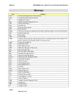
Страница 130: ... describes the PC AT compatible region of battery backed 128 bytes of memory which normally resides on the server board CSB5 Legacy I O controller hub DCD Data Carrier Detect DMA Direct Memory Access DMTF Distributed Management Task Force ECC Error Correcting Code EMC Electromagnetic Compatibility EMP Emergency management port EPS External Product Specification ESCD Extended System Configuration D...

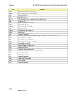
Страница 131: ...lti Bit Error Ms milliseconds MSB Most Significant Bit MTBF Mean Time Between Failures Mux multiplexor NIC Network Interface Card NMI Non maskable Interrupt OEM Original equipment manufacturer Ohm Unit of electrical resistance P32 A 32 bit PCI Segment P64 B Full Length 64 66 MHz PCI Segment P64 C low profile 64 66 MHz PCI Segment PBGA Pin Ball Grid Array PDB Power Distribution Board PEF Platform E...

Страница 132: ...tem event log SERIRQ Serialized Interrupt Requests SERR System Error SM Server Management SMI Server management interrupt SMI is the highest priority nonmaskable interrupt SMM System Management Mode SMS System Management Software SNMP Simple Network Management Protocol SPD Serial Presence Detect SSI Server Standards Infrastructure SSU Server Setup Utility TPS Technical Product Specification UART U...

Страница 133: ...Revision 2 2 www pcisig org ATI RAGE XL Graphics Controller Specifications Technical Reference Manual Rev 2 01 www ati com SE7500CW2 BIOS External Product Specification rev 1 01 SE7500CW2 Baseboard External Product Specification 1 01 Windbond 83627HF Super I O Controller Technical Reference rev 1 0 www Windbond com 1 Please contact your Intel field person for informaiton on how to obtain this docu...

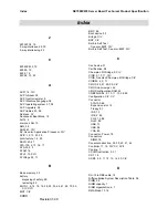
Страница 134: ... BIOS 1 5 15 18 19 28 29 33 44 47 48 70 90 CIV CVII BIST CIV BMC 89 Boot device 35 Bridge CIV BSP CIV Built in Self Test See also BIST CIV Built in Self Test See also BIST CIV C Cache size 31 Certification 98 Champion I O Bridge 9 CIV CIOB 9 10 11 CIV CIOB See also Champion I O Bridge CIV CIOB20 4 9 11 CMOS 44 47 90 99 CIV CMOS clear jumper 44 CMOS configuration RAM 44 CNB20HE SL 9 10 11 13 28 29 ...

Страница 135: ...et 68 CIV Front Side Bus 2 FRU CIV FRU See also Field Replaceable Unit CIV G GPIO 9 14 CIV GUID CIV H Hardware Design Guide 43 HDG 43 HE SL 2 4 7 9 10 I I O Bridge 2 ICH3 S 20 ICMB CIV ICMB See also Inter chassis Management Bus CIV IDE interface 12 13 iFLASH 44 IMB CIV IMB bus 9 11 Intel Server Control See also ISC v2 x See also ISC v3 x CIV Intelligent Platform Management Bus See also IPMB CIV Se...

Страница 136: ...ge 12 PDC20267 2 13 16 Peak overshoot 96 PEF CV PERR CV PIO Mode 16 Platform Event Trap CV PME 37 POST 31 33 35 44 47 63 70 CV Power button 36 37 38 Power Distribution Board 78 CV Power management 12 power management controller 12 14 Power Management Interrupt 37 Power switch 37 Power on Self Test See POST 31 33 35 44 47 48 63 70 CV Private Management Bus CV Processor 4 CIV Processor socket 4 80 C...

Страница 137: ...IOS 38 39 42 SMI 35 37 CVI SMM CVI SMS See also Mode Select CVI SNMP CVI Socket370 4 80 South Bridge 9 11 SPD 29 Splash screen 39 43 44 SSU See also System Setup Utility CVI Super I O 2 14 15 32 36 Super I O controller 2 Support circuitry 4 17 SVGA 18 SYSID table 38 System event log 43 70 System fan 3 System Management Mode CVI System Management Software CVI System Setup Utility 33 T Temperature O...

Страница 138: ...Index SE7500CW2 Server Board Technical Product Specification CXXVI Revision 1 40 X Xeon Processor iii Xeon Processor CIII ...

Отзывы: