


Subsystem Details
Intel® Quark™ SE Microcontroller C1000
Platform Design Guide
June 2017
24
Document Number: 334715-004EN
3.2
General Design Guideline Assumptions
The following assumptions pertain to all the subsystems discussed in this chapter:
Package length compensation is needed. The length values are tested and
measured as package-pin-to-package-pin.
The breakout and breaking minimum spacing ratio is 1:1 for all interfaces.
The trace width/intra-spacing for differential pairs and trace width for single-
ended signals depend on the impedance.
For analog signals, it is important to keep the analog ground return path clean
of digital noise to maintain a high signal-to-noise ratio.
Note:
If a specific interface design guide is not available, follow the general guidelines in
this section.
Note:
All routing guidelines in this document are simulated based on the CRB stackup.
Note:
For technical specifications (such as speeds, supported resolutions, and data rates),
please refer to the Intel® Quark™ SE Microcontroller C1000 Datasheet.
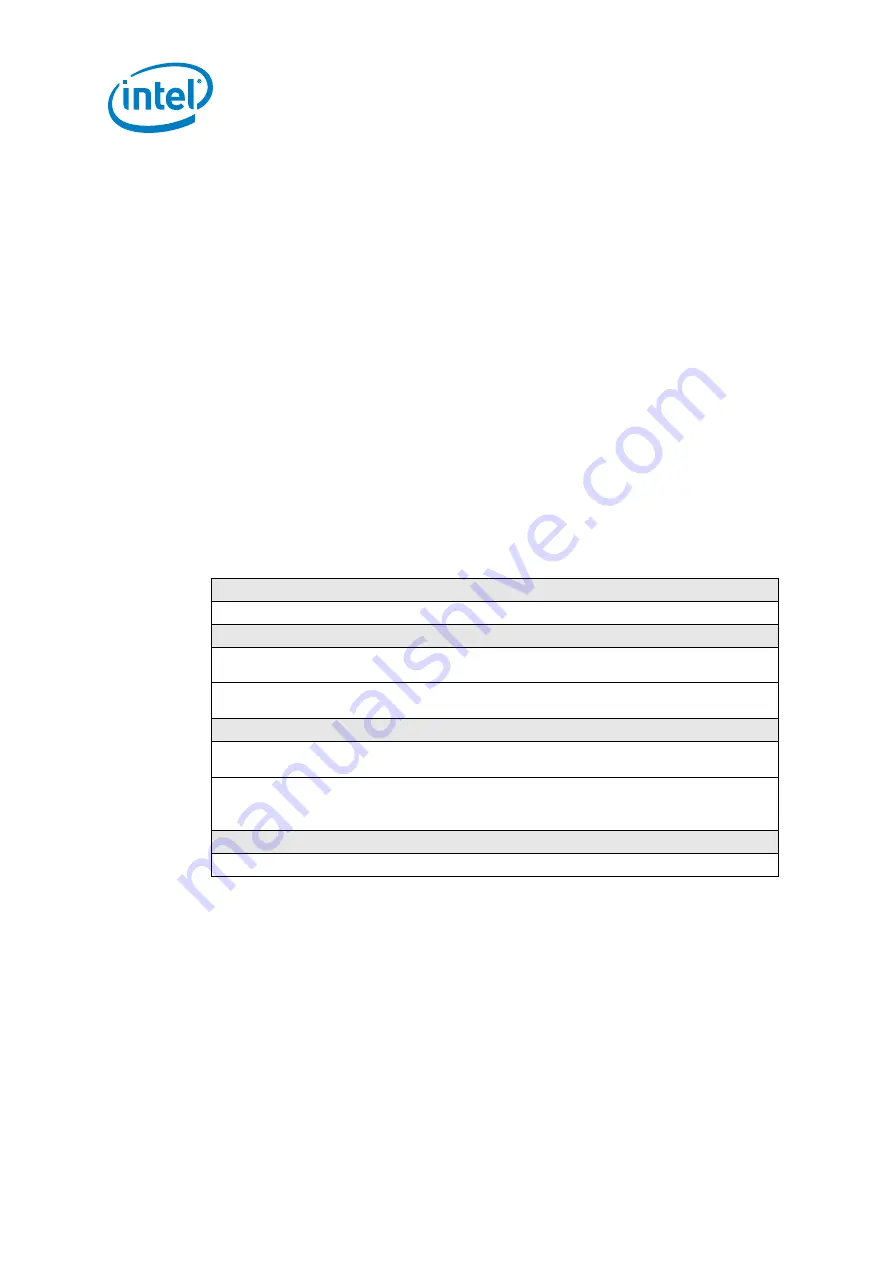
Table 5. Good Layout Practices
Stitching Vias
Provide stitching vias for layer transitions.
Break-in/Break-out Regions
1. If desired trace width cannot be maintained in the break regions, maintain a minimum
trace width of 3.5 mil.
2. If desired trace spacing cannot be maintained in the break regions, maximize the trace
spacing.
Over and Around the voids
1. Avoid routing over the voids and reference plane splits. Consult the SIE if split crossing
cannot be avoided.
2. When going around the voids, maintain a minimum spacing of 1xh between signal trace
and void.
Desirable spacing is 3xh where "h" is the distance to the nearest reference plane.
Lateral Distance to Reference Plane Edge
1. Keep a signal trace 4xh away from the edge of the reference plane.
§


