


System Assumptions
Intel® Quark™ SE Microcontroller C1000
June 2017
Platform Design Guide
Document Number: 334715-004EN
11
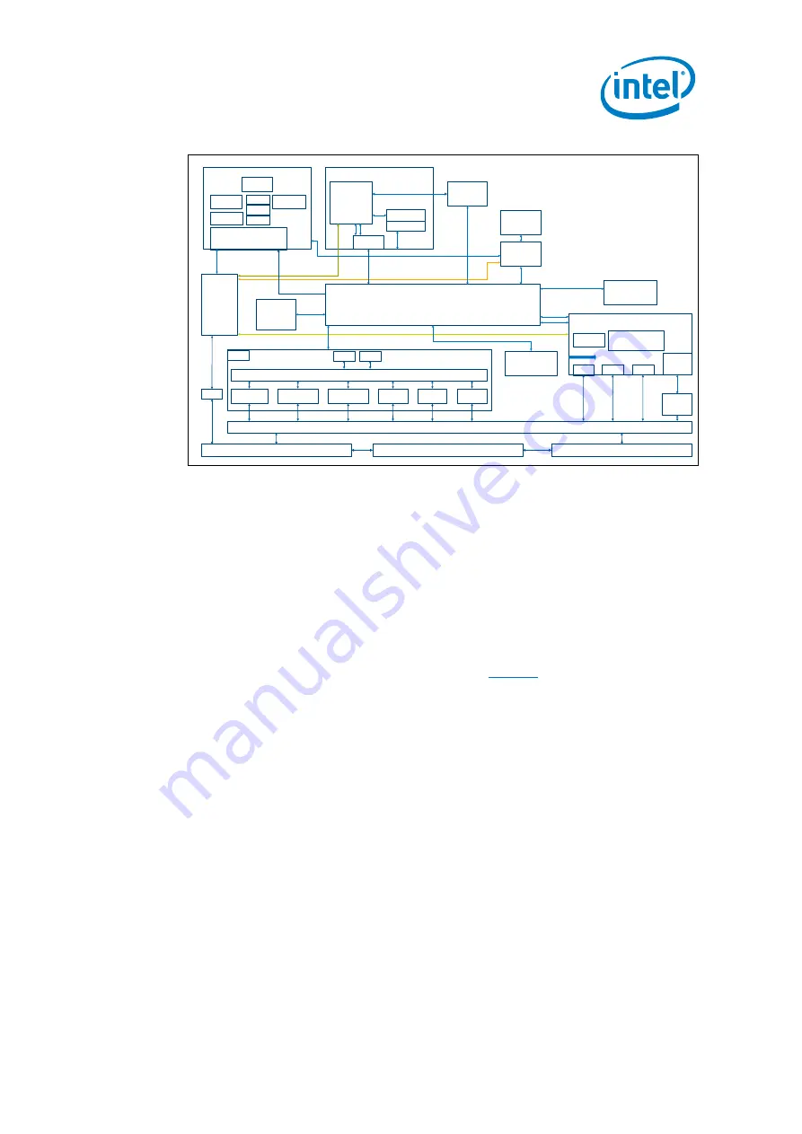
Figure 2. SoC Block Diagram
SPI
GPIO
ADC
Controller
I2C
AHB Fabric
Multi-Channel
DMA
Controller
JTAG/TAP/
DFx Test
Controller(s)
APB Fabric
WDT
RTC
JTAG
Pin Muxing
Digital I/O Pads
Sensor Processor Subsystem
ARC DSP
Core
SAR ADC
USB 1.1 Device
Controller
Interrupts
SRAM
80kB
PERIPH
Comparator HIPs
Analog I/O Pads
Flash
192kBx2
OTP
Flash
PWM
(Timer)
I2S + Fifo
Memories
2 x UART
SPI (2 Master & 1
Slave)
I2C (2 Master &
1 Slave)
AHB Bridge
Host Processor
Processor
Core
Local APIC
Interrupts
I/O APIC
System Control
Interface & Registers
System Control SubSystem
VRs/
LDOs
Interrupt
Routing
Wake Event
Routing
OSC
PLL
CRU
PMU
GPIO
DCCM
Memory
Pattern Matching
Engine
2.1.1
PCB Technology and Stackup
The system uses the PCB technology of a standard interconnect, Type 3, 6-layer
board, with no blind or buried vias. The BGA package also supports a standard
interconnect, Type 3, 4-layer PCB design technology. It is important to note that
variations in the stackup of a motherboard, such as changes in the dielectric height,
trace widths, and spacing, can impact the impedance or loss and jitter
characteristics of all interfaces. Such changes may be intentional or may be a result
of variations in the manufacturing process. In either case, they must be properly
considered when designing interconnects. This design guide applies the CRB PCB
stackup and trace width/spacing that is shown in
Note:
All routing guidelines in this document are simulated based on the CRB stackup.
2.1.2
PCB Technology Considerations
The typical values, including the design and material tolerances, are centered on a
nominal single line impedance specification of 50
𝛺 ± 15%
for microstrip. Many
interfaces specify a different nominal single-ended impedance. For more details on
the nominal trace width to meet those impedance targets, refer to the individual
interface section.
Follow these general stackup recommendations:
Microstrip layers are assumed to be built from 1/2oz. foil, plated up nominally
another 1 oz. However, the defined trace thickness range allows for significant
process variance around this nominal.
Dual stripline is assumed to be built from 1 oz. copper, based on the Intel®
Quark™ SE Microcontroller C1000 layout layers 2/3/4/5.


