


Folders
Files
tb_checker/tb_serial_check_counter.v
tb_checker/tb_serial_descrambler.v
tb_checker/tb_tx_clkout_check.v
vid_pattgen/sdi_ii_colorbar_gen.v
(for parallel loopback design)
vid_pattgen/sdi_ii_ed_vid_pattgen.v
(for parallel loopback design)
vid_pattgen/sdi_ii_makeframe.v
(for parallel loopback design)
vid_pattgen/sdi_ii_patho_gen.v
(for parallel loopback design)
xcelium
/xcelium_sim.sh
1.2. Generating the Design
Configure the SDI II Intel FPGA IP parameter editor in the Intel Quartus
®
Prime
software to generate the design examples.
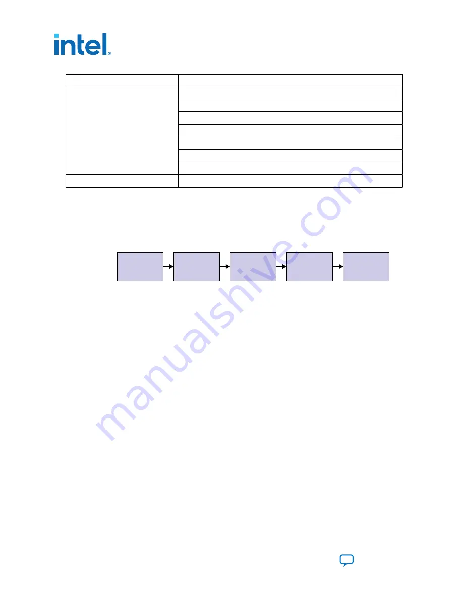
Figure 3.
Generating the Design Flow
Start Parameter
Editor
Specify IP Variation
and Select Device
Select
Design Parameters
Specify
Example Design
Initiate
Design Generation
1. Create an empty project targeting Intel Agilex device family and select the desired
device.
2. In the IP Catalog, locate and double-click SDI II Intel FPGA IP. The IP
Parameter Editor window appears.
3. Specify a top-level name for your custom IP variation. The parameter editor saves
the IP variation settings in a file named
<your_ip>.ip
or
<your_ip>.qsys
.
4. On the Design Example tab, select the desired parameter for the design
example. Select Simulation to generate the testbench, and select Synthesis to
generate the hardware design example.
5. For Target Development Kit, select the relevant FPGA development kit. You may
change the target device using the Change Target Device parameter if your
board revision does not match the grade of the default targeted device.
6. Click Generate Example Design button to initiate the design generation.
1. F-Tile SDI II Intel
®
Agilex
™
FPGA IP Design Example Quick Start Guide
710496 | 2022.01.28
F-Tile SDI II Intel
®
Agilex
™
FPGA IP Design Example User Guide
6


