5137ch02.fm
Draft Document for Review October 14, 2014 10:19 am
42
IBM Power Systems E870 and E880 Technical Overview and Introduction
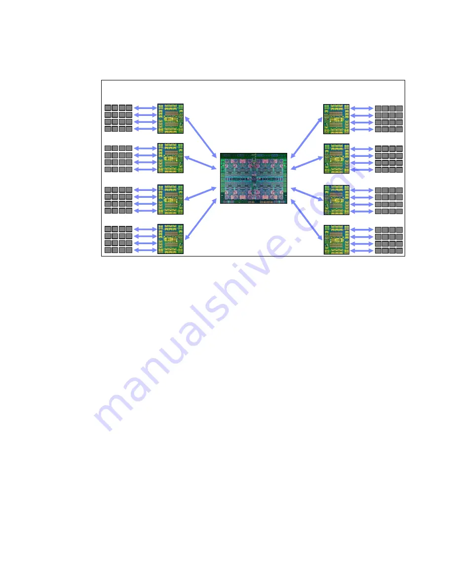
Figure 2-9 gives a simple overview of the POWER8 processor memory access structure in
the Power E870 and Power E880.
Figure 2-9 Overview of POWER8 memory access structure
2.2.5 On-chip L3 cache innovation and Intelligent Cache
Similar to POWER7 and , the POWER8 processor uses a breakthrough in material
engineering and microprocessor fabrication to implement the L3 cache in eDRAM and place it
on the processor die. L3 cache is critical to a balanced design, as is the ability to provide good
signaling between the L3 cache and other elements of the hierarchy, such as the L2 cache or
SMP interconnect.
The on-chip L3 cache is organized into separate areas with differing latency characteristics.
Each processor core is associated with a fast 8 MB local region of L3 cache (FLR-L3) but also
has access to other L3 cache regions as shared L3 cache. Additionally, each core can
negotiate to use the FLR-L3 cache that is associated with another core, depending on the
reference patterns. Data can also be cloned and stored in more than one core’s FLR-L3
cache, again depending on the reference patterns. This
Intelligent Cache management
enables the POWER8 processor to optimize the access to L3 cache lines and minimize
overall cache latencies.
Figure 2-6 on page 37 and Figure 2-7 on page 38 show the on-chip L3 cache, and highlight
one fast 8 MB L3 region closest to a processor core.
The benefits of using eDRAM on the POWER8 processor die is significant for several
reasons:
Latency improvement
A six-to-one latency improvement occurs by moving the L3 cache on-chip compared to L3
accesses on an external (on-ceramic) ASIC.
Bandwidth improvement
A 2x bandwidth improvement occurs with on-chip interconnect. Frequency and bus sizes
are increased to and from each core.
POWER8
Processor
Memory
Buffers
DRAM
Chips
Memory
Buffers
DRAM
Chips


