Rev. 1.10
70
October 23, 2020
Rev. 1.10
71
October 23, 2020
BC66F5652
2.4GHz RF Transceiver A/D Flash MCU
BC66F5652
2.4GHz RF Transceiver A/D Flash MCU
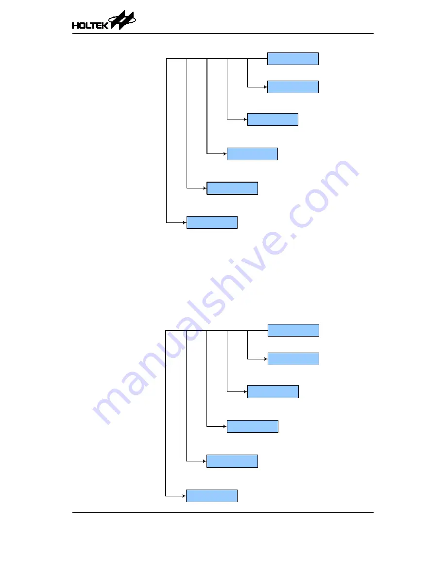
FAST Mode
SLOW Mode
CKS2~CKS0=111
SLEEP Mode
FHIDEN=0, FSIDEN=0
HALT instruction is executed
IDLE0 Mode
FHIDEN=0, FSIDEN=1
HALT instruction is executed
IDLE1 Mode
FHIDEN=1, FSIDEN=1
HALT instruction is executed
IDLE2 Mode
FHIDEN=1, FSIDEN=0
HALT instruction is executed
SLOW Mode to FAST Mode Switching
In SLOW mode the system clock is derived from f
SUB
. When system clock is switched back to the
FAST mode from f
SUB
, the CKS2~CKS0 bits should be set to “000”~“110” and then the system
clock will respectively be switched to f
H
~f
H
/64.
However, if f
H
is not used in SLOW mode and thus switched off, it will take some time to re-
oscillate and stabilise when switching to the FAST mode from the SLOW Mode. This is monitored
using the HXTF bit in the HXTC register or the HIRCF bit in the HIRCC register. The time duration
required for the high speed system oscillator stabilization is specified in the System Start Up Time
Characteristics.
FAST Mode
SLOW Mode
CKS2~CKS0=000~110
SLEEP Mode
FHIDEN=0, FSIDEN=0
HALT instruction is executed
IDLE0 Mode
FHIDEN=0, FSIDEN=1
HALT instruction is executed
IDLE1 Mode
FHIDEN=1, FSIDEN=1
HALT instruction is executed
IDLE2 Mode
FHIDEN=1, FSIDEN=0
HALT instruction is executed


