56
CDR-830
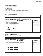
[Procedure]
1. Press the AUTO/MANUAL key and shift to the RFOM Offset Adjustment.
2. Monitor the RFDC waveform with VC.
2. Adjust the JOG key so that RFDC offset becomes zero.
3. Press the ENTER key to register the adjustment.
6.7.4 RFOM Offset Adjustment
0 mV
±
30 mV
CN102-pin 2 (RF)
Test Point
Adjustment Value
Optimizing DC offset voltage of RFDC output circuit when playing back.
Focus-in does not function, incapable of searching, or track jumping.
Purpose
Symptom when Out of Adjustment
Adjustment method
FL Indication
CN102
RF
VC
2
6
10: 1 prove
Oscilloscope
[Procedure]
1. Press the AUTO/MANUAL key and shift to the MPP Offset Adjustment.
2. Monitor the MPP waveform with VC.
2. Adjust the JOG key so that MPP offset becomes zero.
3. Press the ENTER key to register the adjustment.
6.7.5 MPP Offset Adjustment
0 mV
±
50 mV
CN102-pin 4 (MPP)
Test Point
Adjustment Value
Playback does not function, incapable of searching, or track jumping.
Optimizing DC offset voltage of main signal output circuit.
Purpose
Symptom when Out of Adjustment
Adjustment method
FL Indication
CN102
MPP
VC
4
6
10: 1 prove
Oscilloscope
Содержание BurnIT CDR-830
Страница 42: ...CDR 830 42 A B C D 1 2 3 4 1 2 3 4 PNP1478 A IC404 Q405 Q404 Q403 IC801 IC405 IC601 AUDIO ASSY D SIDE B D...
Страница 45: ...CDR 830 45 A B C D 5 6 7 8 5 6 7 8 G IC701 IC702 IC706 CN601 D SIDE A SIDE B...
Страница 71: ...71 CDR 830 Pin Function 2 5...
Страница 72: ...72 CDR 830 Pin Function 3 5...
Страница 73: ...73 CDR 830 Pin Function 4 5...
Страница 74: ...74 CDR 830 Pin Function 5 5...
Страница 78: ...78 CDR 830 AK8567 CD R CORE PCB ASSY IC101 RF Processor Pin Function 1 2...
Страница 79: ...79 CDR 830 Pin Function 2 2...
Страница 82: ...82 CDR 830 1 FL TUBE Grid Assignment Pin Connection PEL1101 OPERATING ASSY V701 7 2 2 DISPLAY...
Страница 83: ...83 CDR 830 Anode Connection...
Страница 89: ...CDR 830 89 ORDER NO RRV2408M T ZZR DEC 2000 Printed in Japan...


