CON1
Q1
CON2
Q2
VDC-
CON4
CON3
L
OUT
400V DC
+
VDC+
CON7
CON6
VSW
CON5
+5V
0V
PWM
INPUT
(J7)
V
DS
I
L
I
SW
V
GL
+6V
0V
V
DS
V
GL
I
L
t0
t1 t2 t3
T
ON1
Double pulse test allows easy evaluation of device switching performance at high voltage/current
without the need of actually running at high power. It can also be used for switching loss (Eon/Eoff)
measurement and other switching characterization parameter test.
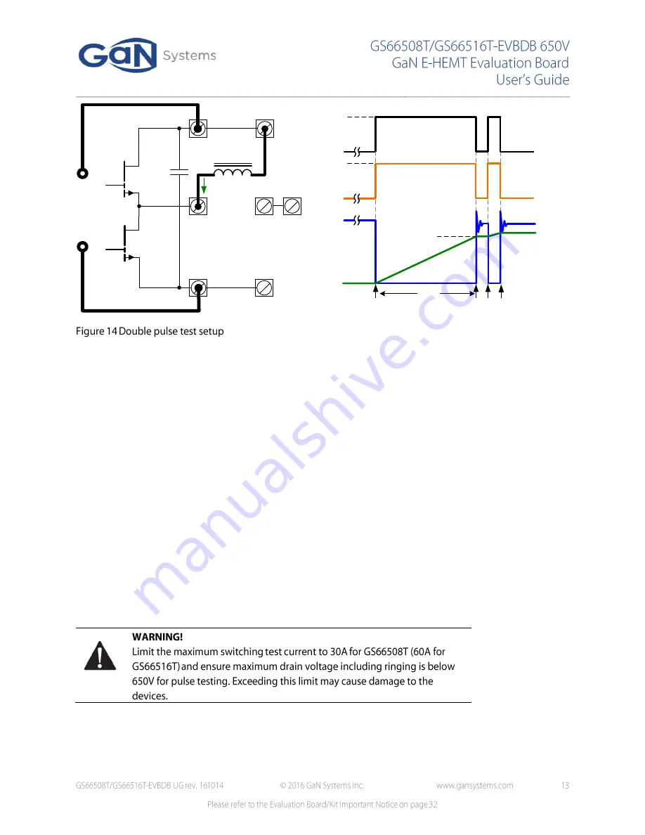
The circuit configuration and operating principle can be found in Figure 14:
1.
The output inductor is connected to the VDC+.
2.
At t0 when Q2 is switched on, the inductor current starts to ramp up until t1. The period of first
pulse Ton1 defines the switching current I
SW
= (V
DS
*T
ON1
) / L.
3.
t1-t2 is the free wheeling period when the inductor current I
L
forces Q1 to conduct in reverse.
4.
t1 (turn-off) and t2 (turn-on) are of interest for this test as they are the hard switching trasients for
the half bridge circuit when Q2 is under high switching stress.
5.
The second pulse t2-t3 is kept short to limit the peak inductor current at t3.
The double pulse signal can be generated using programmable signal generaotor or microcontroller/DSP
board. As this test involves high switching stress and high current, it is recommended to set the double
pulse test gate signal as single trigger mode or use long repetition period (for example >50-100ms) to void
excess stress to the switches. Q1 can be kept off during the test or driven synchronously (J4 set to OFF or
INT_INV) and Q2 is set to INT (or EXT position if PWM signal is from J5).
Содержание GS66502B-EVBDB
Страница 9: ...GaNPX T GaNPX T FR4 PCB Heatsink M3 Screw Lock Washter Insulated bushing TIM...
Страница 17: ......
Страница 19: ...A T M search coaxial current shunt SDN 414 10 0 1 is installed for switching loss measurement as shown below...
Страница 23: ......
Страница 25: ......
Страница 26: ...Top Layer Mid Layer 1 Mid Layer 2 Bottom Layer...
Страница 29: ...Assembly Top Assembly Bottom...
Страница 32: ......


