


Pub. 42004-392G
M
ODEL
LE200-RM
R
ACK
-M
OUNT
P
AGE
/P
ARTY
®
L
INE
E
XTENDER
P
AGE
20 of 56
e:\standard ioms - current release\42004 instr. manuals\42004-392g.doc
09/14
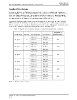
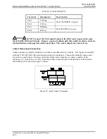
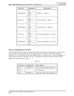
T1/E1 Receiver Equalization Gain Limit
This option allows the user to compensate for diminishing signal intensity over the data line by adjusting
the sensitivity of the receiver. By setting the Receive Equalizer Gain Limit, very long copper lines can be
utilized. DIP switch SW2 position 4 on the Main PCBA selects the parameter. Refer to Figure 6 for the
location of SW2 on the Main PCBA and Table 19 below for setting details.
Table 19. Receive Equalizer Gain Limit Setting on Main PCBA
SW2-4
Receive Equalization Gain Limit
T1 Mode
E1 Mode
Open (up)*
−
36 dB (long haul)
−
12 dB (short haul)
Closed (down)
−
15 dB (limited long haul)
−
43 dB (long haul)
N
OTES
:
1. Changes to this parameter take effect without cycling power.
2.
*Indicates
default
position.
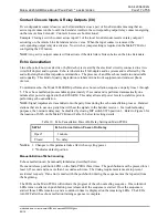
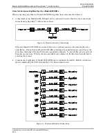
T1/E1 Clock Source
For each pair of Line Extenders, one Line Extender must be the master clock source. The other unit must
be the slave. The slave unit receives the clock from the master. DIP switch SW3 positions 1 and 2 on the
Main PCBA selects T1/E1 clock parameters. Refer to Figure 6 for the location of SW3 on the Main PCBA
and Table 20 below for setting details.
Table 20. Master Clock Setting on Main PCBA
SW3-1 SW3-2 Clock
Source
Open*
Open*
LE200-RM is the T1/E1 Master (generates the T1/E1 clock).
Closed
Closed LE200-RM is the T1/E1 Slave (receives the T1/E1 clock from master).
N
OTES
:
1. Changes to this parameter take effect
after cycling power
.
2.
*Indicates
default
position.