


66
Chapter 9
DSPI: Deserial Serial Peripheral Interface
1.
Introduction
There are three identical DSPI modules (0…2) in this microcontroller for using SPI serial bus
protocol in order to communicate with external devices.
1.1.
SPI Protocol Description
The Serial Peripheral Interface (SPI) is a synchronous serial communication bus in which there
is only one master and at least one slave. This bus can operate in full-duplex mode, transmitting
and receiving at the same time. There are at least four logical signals but in a single slave
situation only three of them can be enough.
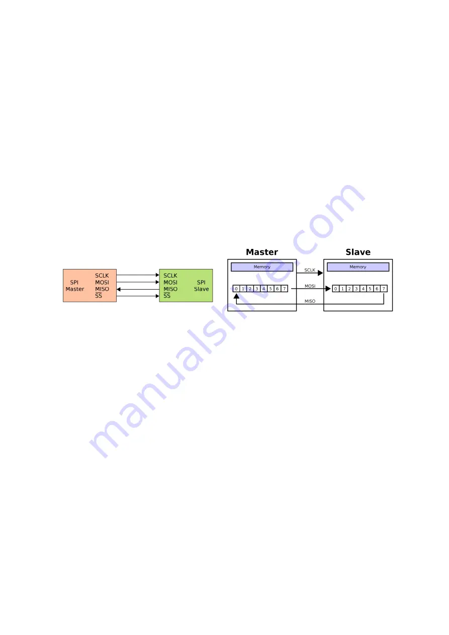
Figure 84 : SPI Master/Slave Illustrations
These signals are:
SCLK (or SCK in DSPI): a clock generated by the master to synchronise the exchange,
MOSI (or SOUT in DSPI Master, SIN in DSPI Slave): Master Output Slave Input, data sent
by the master
MISO(or SIN in DSPI Master, SOUT in DSPI Slave): Master Input Slave Output, data sent
by the slave
SS (or CS in DSPI): Slave Select (Chip Select), selection of a slave.
In MOSI/MISO naming convention, MOSI of the master is connected to MOSI of the slave and
similarly their MISO are connected together, but in SOUT/SIN naming convention (DSPI’s case),
SOUT is connected to SIN and SIN to SOUT.
There is a shift register in both master and slave (usually 8-bit) and following the clock ticking of
the master, these registers are rotated until the data in them is completely exchanged.
There are many parameters about details of this transmission that can be configured, and both
master and slave has to have similar configurations for valid communication like the frame size
(shift register’s size). The master’s clock frequency is also called the SPI Baud Rate, image of the
data transmission speed, can be selected on a wide range on values, and this clock’s polarity
(CPOL) can be selected. Another important parameter is the clock phase (CPHA) with defines
the edge where the data is sampled.
Содержание MPC5604B
Страница 1: ...LAAS CNRS Quick Start to MPC5604B Embedded Development Sahin Serdar 21 06 2013...
Страница 31: ...Figure 33 INTC SW HW mode comparison Freescale Tutorial...
Страница 87: ......
Страница 132: ......
Страница 133: ...127 Appendix 2 Pad Configurations...
Страница 134: ......
Страница 135: ......
Страница 136: ......
Страница 137: ......
Страница 138: ......
Страница 139: ......
Страница 140: ......
Страница 141: ...Appendix 3 Peripheral input pin selection...
Страница 142: ......
Страница 143: ...137 Appendix 4 Interrupt Vector Table...
Страница 144: ......
Страница 145: ......
Страница 146: ......
Страница 147: ......
Страница 148: ...Appendix 5 I C Baud Rate Prescaler Values...
Страница 149: ......
Страница 150: ......


