


MCF5282 User’s Manual Errata, Rev. 15
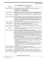
Errata for Revision 1.0
Freescale Semiconductor
10
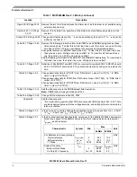
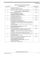
Figure 33-5/33-16
Replace Figure 33-5, ‘SDRAM Read Cycle’ with the figure below.
Figure 33-5. SDRAM Read Cycle
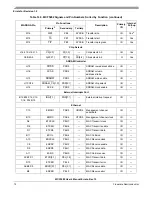
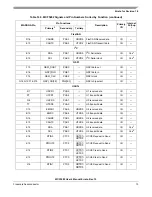
Table 14-3/14-11
Change ‘Internal Pull-Up’ column to pull-up indications in the table below.
Table 14-3. MCF5282 Signals and Pin Numbers Sorted by Function
MAPBGA Pin
Pin Functions
Description
Primary
I/O
Internal
Pull-up
1
Primary
2
Secondary
Tertiary
Reset
R11
RSTI
—
—
Reset in
I
Yes
P11
RSTO
—
—
Reset out
O
—
Clock
T8
EXTAL
—
—
External clock/crystal in
I
—
Table 4. MCF5282UM Rev 1.0 Errata (continued)
Location
Description
A[23:0]
SRAS
D[31:0]
ACTV
NOP
SDRAM_CS[1:0]
READ
Column
CLKOUT
0
DRAMW
BS[3:0]
1
2
3
4
5
6
7
8
9
10
11
12
13
D1
D2
D4
D6
D5
D4
1
DACR[CASL] = 2
SCAS
1
NOP
D4
Row
D3
PRE


