


2010-06-30
Page 20 of 42
IT430_Tech_doc.doc
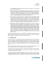
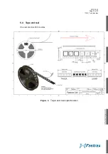
Figure 2
Suggested ON_OFF Hibernate control timing diagram.
NOTE
Do not generate multiple ON_OFF interrupts less than 1 sec
intervals. Especially filter out multiple pulses generated by a
mechanical switch bounce.
4.5 Reset input
The RESET_N (active low) signal provides external override of the internally generated power
up/down reset. Normally external control of RESET_N is not necessary. When power supply
VDD may be abruptly removed, suggestion is to use externally generated reset by means of
external VDD voltage monitor.
When RESET_N signal is used, it will force volatile RAM data loss (e.g. ROM patch code). Non-
Volatile Backup RAM content is not cleared and thus fast TTFF is possible after reset. The input
has internal pull up resistor 86 kohm typ. and leave it not connected (floating) if not used.
4.6 Antenna input
The module supports passive and active antennas. The antenna input RF_IN impedance is 50
ohms and it provides also a bias supply low-pass filtered form VDD_ANT supply. Note that
antenna input is ESD sensitive. With passive antennas the ESD performance can be improved
by connecting VDD_ANT supply input to GND.
NOTE
With Passive antennas leave VDD_ANT not connected or
connect to GND.
Содержание IT430
Страница 24: ...2010 06 30 Page 24 of 42 IT430_Tech_doc doc Figure 3 Dimensions ...
Страница 38: ...2010 06 30 Page 38 of 42 IT430_Tech_doc doc 7 3 Circuit drawing ...
Страница 39: ...2010 06 30 Page 39 of 42 IT430_Tech_doc doc 7 4 Assembly drawing Top side 7 5 Artwork layer 1 Top ...
Страница 40: ...2010 06 30 Page 40 of 42 IT430_Tech_doc doc 7 6 Artwork layer 2 7 7 Artwork layer 3 ...
Страница 41: ...2010 06 30 Page 41 of 42 IT430_Tech_doc doc 7 8 Artwork layer 4 Bottom ...


