


2010-06-30
Page 15 of 42
IT430_Tech_doc.doc
used.
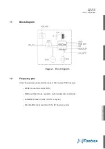
13
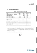
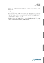
RTS_N
S,C,B,
PU(a)
S,C,B, PU
HZ
- GPIO7
- SPI_SS_N slave SPI chip select
(CS#), active low
- UART_RTS_N UART ready to
send (RTS), active low
- Host port boot strap, see 4.3
Can be left unconnected when not
used.
14
GND
G
G
G
Ground
15
TX
S,C,B
HZ
HZ
- SPI_DO slave SPI data output
(MISO)
- UART_TX UART data transmit
(TX)
- I2C_CLK I²C bus clock (SCL)
16
RX
S,C,B
HZ
HZ
- SPI_DI slave SPI data input
(MOSI)
- UART_RX UART data receive
(RX).
Must be driven by host or
use external pull up resistor (UART
RX).
- I2C_DIO I²C bus data (SDA)
17
ON_OFF
S,C,B
S,C,B
S,C,B
Power control input used to
command the module On
(Navigation) or Off (Hibernate).
Must be driven by the host.
18
GND
G
G
G
Ground
19
GND
G
G
G
Ground
20
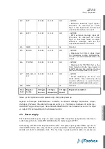
TM
S,C,B
S,C,B
HZ
- GPIO5
- Time mark output signal
(default
1PPS)
-
Optionally
GPS_ON,
power
control output signal for e.g.
external LNA bias control.
- Optionally RTC_CLK, buffered
RTC clock output.
Can be left
unconnected when not used.
21
WAKEUP
C,O
C,O
C,O
Wakeup output for control of
external regulator, e.g. battery to
1.8V for the VDD supply input
when full power mode is entered.
Can be used also externally for
active antenna bias control, active
high = high current/bias on.
Can
be left unconnected when not
used.
Содержание IT430
Страница 24: ...2010 06 30 Page 24 of 42 IT430_Tech_doc doc Figure 3 Dimensions ...
Страница 38: ...2010 06 30 Page 38 of 42 IT430_Tech_doc doc 7 3 Circuit drawing ...
Страница 39: ...2010 06 30 Page 39 of 42 IT430_Tech_doc doc 7 4 Assembly drawing Top side 7 5 Artwork layer 1 Top ...
Страница 40: ...2010 06 30 Page 40 of 42 IT430_Tech_doc doc 7 6 Artwork layer 2 7 7 Artwork layer 3 ...
Страница 41: ...2010 06 30 Page 41 of 42 IT430_Tech_doc doc 7 8 Artwork layer 4 Bottom ...


