


2010-06-30
Page 14 of 42
IT430_Tech_doc.doc
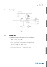
4
CONNECTIVITY
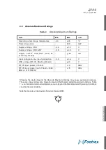
4.1 Signal assignments
The I/O signals are available as soldering (castellated) pads on the bottom side of the module.
These pads are also used to attach the module on the motherboard. All I/O signal levels are 1.8V
CMOS compatible and inputs are 3.6V tolerable. All unconnected I/O signals can be left
unconnected when not used, unless instructed to use external pull up/down resistor.
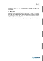
Table 3
Connections
Con
tact
Signal
name
I/O type
Full on
I/O type
Hibernate
I/O type
Reset
Signal description
1
VDD
P,I
P,I
P,I
Power supply input +1.8V nom.
De-couple
externally
with
e.g.
4.7uF low ESR ceramic capacitor.
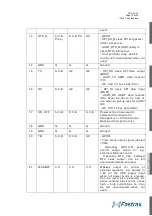
2
DR_I2C_D
IO
S,C,B
S,C,B
HZ
- GPIO0
- Dead reckoning I
2
C host bus data
(SDA).
Use
external
pull
up
resistor when bus is used.
Can be
left unconnected when not used.
3
VDD_ANT
P,I
P,I
P,I
Antenna bias power supply input
up to +/-5.5V.
De-couple signal
further externally, see Application
Circuit Diagram.
4
GND
G
G
G
Ground
5
GND
G
G
G
Ground
6
RF_IN
A,I,O
A,I,O
A,I,O
Analog Antenna input (50 ohm),
Antenna
bias
voltage
output
(filtered from VDD_ANT)
7
GND
G
G
G
Ground
8
GND
G
G
G
Ground
9
GND
G
G
G
Ground
10
GND
G
G
G
Ground
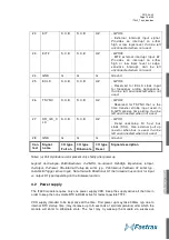
11
CTS_N
S,C,B,
PD(a)
S,C,B, PD
HZ
- GPIO6
- SPI_CLK slave SPI clock input
(CLK)
- UART_CTS_N UART clear to
send (CTS), active low
- Host port boot strap, see 4.3
Pull up externally for UART.
12
RESET_N
C,I,PU
C,I,PU
C,I,PU
External reset input, active low.
Can be left unconnected when not
Содержание IT430
Страница 24: ...2010 06 30 Page 24 of 42 IT430_Tech_doc doc Figure 3 Dimensions ...
Страница 38: ...2010 06 30 Page 38 of 42 IT430_Tech_doc doc 7 3 Circuit drawing ...
Страница 39: ...2010 06 30 Page 39 of 42 IT430_Tech_doc doc 7 4 Assembly drawing Top side 7 5 Artwork layer 1 Top ...
Страница 40: ...2010 06 30 Page 40 of 42 IT430_Tech_doc doc 7 6 Artwork layer 2 7 7 Artwork layer 3 ...
Страница 41: ...2010 06 30 Page 41 of 42 IT430_Tech_doc doc 7 8 Artwork layer 4 Bottom ...


