Page 10
Epson Research and Development
Vancouver Design Center
S1D13505
13505CFG Configuration Program
X23A-B-001-04
Issue Date: 01/03/29
Memory Tab
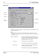
The Memory tab contains settings that control the configuration of the DRAM used for the
S1D13505 display buffer.
Note
The DRAM memory type and access time determines the optimal memory clock
(MCLK). See “Clocks Tab” on page 12 for an explanation on how to determine the op-
timal memory clock.
Memory Configuration
These four settings must be configured based on the
specification of the DRAM being used. For each of the
following settings refer to the DRAM manufacturer’s
specification unless otherwise noted.
Access Time
Selects the access time of the DRAM.
The S1D13505 evaluation boards use 50ns DRAM.
Memory Type
Selects the memory type, either Extended Data Out
(EDO) or Fast Page Mode (FPM).
The S1D13505 evaluation boards use EDO DRAM.
Access Time
Memory Type
Refresh Time
Suspend Mode
Installed Memory
WE# Control
Memory
Performance


