3. Terminal description
RX8130CE
Jump to
ETM50E-07
Seiko Epson Corporation
7
3. Terminal description
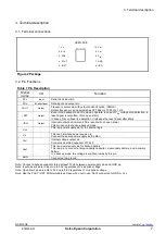
3.1. Terminal connections
RX8130CE
1. V
IO
10. V
BAT
2. SCL
9. V
OUT
3. SDA
8. V
DD
4. FOUT
7. GND
5. /RST
6. /IRQ
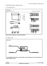
Figure 2 Package
3.2. Pin Functions
Table 1 Pin Description
Signal
name
I/O
Function
SCL
Input
Serial clock input pin.
SDA
Bi-directional
Data input and output pin.
FOUT
Output
Frequency output pin with output control function. (CMOS)
Output frequency can be selected as 32.768k Hz, 1024 Hz, 1 Hz.
/ RST
Output
Even in the backup mode, this pin can operate. In case of V
DD
voltage drop detection, a
reset signal is outputted. (N-ch open drain)
In case of V
DD
voltage rise detection, it releases the reset signal after 60ms.
/ IRQ
Output
Interrupt output by Alarm and Timer events.(N-ch open drain)
This pin can output even a backup mode.
V
DD
This is a power-supply pin for the internal logic.
V
I
O
This is an interface power supply pin.
Connect the same power supply as the MCU.
V
OUT
Internal voltage output pin.
Connect smoothing capacitor of 1.0uF
V
BAT
This is a power supply pin for backup battery.
This is a pin to connect a large-capacity capacitor, a secondary battery, and a primary
battery.
In a backup mode, the voltage is supplied inside by this pin.
GND
Connected to a ground.
Note: Connect a bypass
capacitor rated at least 0.1μF between power supply pins and GND pin.
Note: Input pins are able to input up to 5.5V regardless of V
IO
applied voltage.
Note: Open drain pins are able to Pull-up to 5.5V regardless of V
IO
applied voltage.
Note: Use the FOUT, /RST, /IRQ terminals as Open when not in use. Don't connected to GND or V
DD


