background image

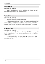
Select PPAGE

Syntax: P [page]

Select a program page (PPAGE). This page will become visible in

the 16KB page window from $8000 to $BFFF.

Erase Flash

Syntax: X [page]

Erase one page (16KB) of Flash memory.

If page is not specified, the whole Flash memory (ex. monitor code

space) will be erased after user confirmation. To remove (erase) the
monitor code, a BDM tool such as ComPOD12/StarProg is required.

Erase EEPROM

Syntax: Y [sadr]

Erase one sector (double word = 4 byte) of EEPROM memory. The

sector is specified by it's starting address sadr (bits 0 and 1 of sadr are
"don't care").

If sadr is not specified, the whole EEPROM will be erased after

user confirmation.

S12compact

44

Содержание S12compact

Страница 1: ...S12compact Hardware Version 1 10 User Manual July 4 2008...

Страница 2: ...ial hardware and firmware In no event shall the manufacturer or its supplier be liable for any damages whatsoever including without limitation damages for loss of business profits business interruptio...

Страница 3: ...ntegrated A D Converter 15 Operating Modes BDM Support 14 Clock Generation and PLL 13 Reset Generation 12 Controller Core Power Supply 12 Schematic Diagram 12 6 Circuit Description 11 5 Mechanical Dim...

Страница 4: ...d EEPROM 38 Autostart Function 38 Serial Communication 38 8 TwinPEEKs Monitor 37 Additional Information on the Web 37 Startup Code 37 Behaviour after Reset 37 7 Application Hints 36 Bus Interface 34 C...

Страница 5: ...full 16 bit data paths throughout An integrated PLL circuit allows adjusting perfor mance vs current consumption according to the needs of the user application In addition to the on chip controller fu...

Страница 6: ...d serial port for IF Modules RS232 RS485 LIN w Indicator LED w Sound Transducer Buzzer w High Speed phys CAN Interface w Reset Button w up to 70 free General Purpose I Os w eight additional digital in...

Страница 7: ...Flash Memory w RS232 Cable Sub D9 w USB Cable only for option USB w set of header connectors two 72 pin male headers w User Manual this document w Schematic Diagrams w CD ROM contains assembler softw...

Страница 8: ...0 connector X2 and PC is simply made using the flat ribbon cable which is in the box w On the PC start a Terminal Program An easy to use Terminal Program is OC Console which is available at no charge...

Страница 9: ...3 Parts Location Diagram Place Plan Component Side User Manual 7...

Страница 10: ...Solder Bridges on the solder side of the PCB S12compact 8...

Страница 11: ...no CAN Bus termination on board closed on board CAN Bus termination active BR3 BUZZ open Port pin PT2 freely available closed PT2 controls buzzer BR4 T1IN open Port pin TXD0 PS1 freely available close...

Страница 12: ...al supply of VREF required closed IC10 delivers reference voltage VREF for the 16 bit A D Converter IC11 and the 16 Bit D A Converter IC12 BR10 DFLE open Port pin MISO1 PH0 freely available closed MIS...

Страница 13: ...reference point 0 0 is located at the south west corner of the PCB The PCB is orientated vertically as shown in the Parts Location Diagram see above All data for holes drills B refer to the center of...

Страница 14: ...he three terminal pairs mentioned above must be decoupled carefully A ceramic capacitor of at least 100nF should be connected directly at each pair C15 C16 C17 It is recommended to add a 10 F electrol...

Страница 15: ...below the level required for proper MCU operation To prevent collisions with the bidirectional RESET pin of the MCU the LVI circuit IC2 has an open drain output In the inactive state it is pulled up h...

Страница 16: ...tray capacitance as possible in respect to XTAL and EXTAL With an OSCCLK of 16MHz the internal bus speed ECLK becomes 8MHz by default To realize higher bus clock rates the PLL has to be engaged The MC...

Страница 17: ...ference Divider SYNR S12_SYNR set up Synthesizer Multiplier the following dummy write has no effect except consuming some cycles this is a workaround for erratum MUCTS00174 mask set 0K36N only CRGFLG...

Страница 18: ...ally usually controlled by a PC based debugging program The 6 pin header X1A uses the suggested standard BDM12 connector layout Connector X1B carries additional MCU signals which are normally not need...

Страница 19: ...12 allows ECLK 6 24MHz 2nd sample time 2 ATD clocks ATD0CTL4 BM_PRS2 BM_PRS0 Func Perform single channel ATD conversion Args channel 0 7 Retn unsigned left justified 10 bit result UINT16 getATD0 UINT8...

Страница 20: ...dule is left at it s default position The initialization sequence just takes care for setting up the EEPROM Clock Divider according to the quartz crystal frequen cy The write function wrSectEETS copie...

Страница 21: ...rase sector dest src ECMD EETS_CMD_SERASE ESTAT BM_CBEIF if ESTAT BM_PVIOL BM_ACCERR return 4 while ESTAT BM_CBEIF 0 program 1st word dest src ECMD EETS_CMD_PROGRAM ESTAT BM_CBEIF if ESTAT BM_PVIOL BM...

Страница 22: ...g C header file File S12CO_LED H V1 00 ifndef __S12CO_LED_H define __S12CO_LED_H Macros define initLED PORTE 0x80 DDRE 0x80 define offLED PORTE 0x80 define onLED PORTE 0x80 define toggleLED PORTE 0x80...

Страница 23: ...annel 2 TIOS BM_2 DDRT BM_2 enable Interrupt for channel 2 TIE BM_2 timer disconnected from PT2 pin TCTL2 BM_OM2 BM_OL2 period is in s void setFreqOut UINT16 period UINT16 tticks tticks period S12_ECL...

Страница 24: ...ines If the RS232 transceiver IC3 is not needed the dedicated MCU pins can be used freely after opening the four solder bridges BR4 BR7 To connect the S12compact to a PC a 10 wire flat ribbon cable ca...

Страница 25: ...5 respectively USB Interface IC15 FT232BM is an USB UART This chip provides a transpa rent conversion from RS232 to USB and back The communication protocol is implemented according to the current USB...

Страница 26: ...normally not required The USB UART has an independent power on reset circuit so normally it does not need an external reset source If BR11 is closed any system reset will temora rily remove the USB de...

Страница 27: ...ins PH 4 6 The decoder chip IC4 activates one of it s eight low active outputs depending on the Port H pattern This provides an economical way to provide up to eight chip selects with a small number o...

Страница 28: ...es a large number of general pur pose I O pins it may be desireable for some applications to keep a number of ports unused This is especially the case if the external bus interface is intended to be u...

Страница 29: ...e set up SPI mode SPI0CR1 BM_SPE BM_MSTR CPOL 0 CPHA 0 latch input data PTH S12CO_SPICS4 PTH S12CO_SPICSH serialize latched data PTH S12CO_SPICS3 abyte xferSPI0 0 PTH S12CO_SPICSH return abyte Real Ti...

Страница 30: ...egno UINT8 result set up SPI mode enable master CPOL 1 CPHA 1 LSB first SPI0CR1 BM_SPE BM_MSTR BM_CPOL BM_CPHA BM_LSBFE transfer data PTH S12CO_SPICS0_RD enable CS0 reading xferSPI0 regno send registe...

Страница 31: ...AIN0 AIN7 The lower limit is ground 0V After opening solder bridge BR9 an external reference voltage can be used instead of IC10 note influence on DAC IC12 The analog inputs AIN0 to AIN7 as well as th...

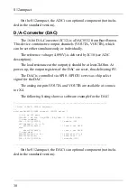
Страница 32: ...ivering 0V The DAC is controlled via SPI0 SPICS1 serves as chip select signal for the DAC The analog outputs VOUTA and VOUTB are available at connec tor X4 The following listing shows a software examp...

Страница 33: ...14 is connected to SPI1 thus being independent from RTC ADC DAC etc which are using SPI0 The SPI1 signals MISO1 MOSI1 SCK1 and the chip select signal SS1 are provided by the MCU s port pins PH0 PH3 No...

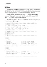
Страница 34: ...upt driven scheme should be preferred See AppNote AN2318 and accompanying software Hard External pull ups on SDA and SCL required Value should be 1k 5k depending on cap bus load Note Adjust IBFD value...

Страница 35: ...er done CAUTION no loop time limit implemented stat IBSR BM_RXAK mask ACK status 0 ACK IBSR BM_IBIF clear IB Intr Flag return stat Func Receive byte from IIC Args ack IIC_ACK IIC_NOACK Retn byte recei...

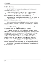
Страница 36: ...no physical drivers are provided on the S12compact They can be added externally if required TTL signals f r CAN1 to CAN3 are available at Port M Please refer to the schematic diagram to see if other f...

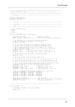
Страница 37: ...e are going to use four 16 bit acceptance filters CAN0IDAC 0x10 set up acceptance filter and mask register 1 7 6 5 4 3 2 1 0 7 6 5 4 3 2 1 0 ID10 ID9 ID8 ID7 ID6 ID5 ID4 ID3 ID2 ID1 ID0 RTR IDE xxx xx...

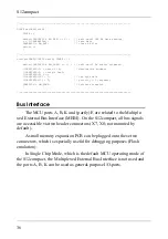
Страница 38: ...BM_TXE0 initiate transfer Bus Interface The MCU ports A B K and partly E are related to the Multiple xed External Bus Interface MEBI On the S12compact all bus signals are accessible via two header co...

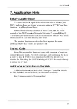
Страница 39: ...immediately after reset The monitor functions are described in a seperate document D Bug12 Reference Guide see product CD Startup Code Every Microcontroller firmware starts with a number of hardware...

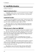
Страница 40: ...byte of the microcontroller s resour ces the type of memory does not matter However for write accesses some rules have to be followed Flash and EEPROM have to be erased before any write attempt Progr...

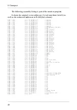
Страница 41: ...t the end of the 64KB memory address range which falls within the protected monitor code space Therefore the application program can not modify the interrupt vectors directly To provide an alternative...

Страница 42: ...3F8E dc w TP_RAMTOP 114 CAN0 receive FFB4 3F91 dc w TP_RAMTOP 111 CAN0 errors FFB6 3F94 dc w TP_RAMTOP 108 CAN0 wake up FFB8 3F97 dc w TP_RAMTOP 105 FLASH FFBA 3F9A dc w TP_RAMTOP 102 EEPROM FFBC 3F9...

Страница 43: ...ndled by a line buffer Valid ASCII codes are in the range from 20 to 7E Backspace 08 will delete the character left of the cursor The ENTER key 0A is used to conclude the input The monitor prompt alwa...

Страница 44: ...fy memory areas which can only be changed on a word by word basis Flash EEPROM In such cases the monitor always awaits and uses 16 bit data To exit the interactive mode simply type Q Additional comman...

Страница 45: ...12 starts at 0x080000 0x20 16KB and ends at 0x0FFFFF 0x40 16 KB 1 Before loading into non volatile memory EEPROM Flash this kind of memory must always be erased Also only word writes can be used in th...

Страница 46: ...e Flash memory ex monitor code space will be erased after user confirmation To remove erase the monitor code a BDM tool such as ComPOD12 StarProg is required Erase EEPROM Syntax Y sadr Erase one secto...

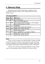
Страница 47: ...FF 0800 1KB of total 4KB EEPROM the area below 0400 is hidden by control registers the top 2048 bytes by the RAM 07FF 0400 Control Registers 03FF 0000 Ressource End Begin Note Due to a mask set erratu...

Отзывы: