Normal Single Chip Mode, which is the most common operating mode
for application code running on the HCS12.
The HCS12 operating mode used for download and debugging is
called Background Debug Mode (BDM). BDM is active immediately
out of reset if the mode pins MODA/MODB/BKGD are configured for
Special Single Chip Mode. This is done by pulling the BKGD pin low
during reset, while MODA and MODB are pulled-down as well.
Because only the BKGD level is different for the two modes, it is
quite easy to change over. However, there is no need to switch the
BKGD line manually via a jumper or solder bridge because this can be
done by a BDM-Pod (such as ComPOD12) attached to connector X1A.
A BDM-Pod is required for BDM-based download and/or debugging
anyway, so it can handle this task automatically, usually controlled by a
PC-based debugging program.
The 6-pin header X1A uses the suggested standard BDM12
connector layout. Connector X1B carries additional MCU signals,
which are normally not needed for BDM12 debugging. Some
debuggers, however, provide additional features, which rely on the
presence of these supplemental signals.
Integrated A/D-Converter
The MC9S12DP512 contains two 10-bit Analog-to-Digital Conver-
ter modules. Each module (ATD0, ATD1) provides eight multiplexed
input channels.
VRH is the upper reference voltage for all A/D-channels. On the
S12compact, VRH is connected to VDDA (5V) through solder bridge
BR1.
After opening BR1, it is possible to use an external reference volta-
ge, which has to be applied to X5/46. For this purpose, the precision
voltage reference IC10 could be used (if present). IC10 delivers 4.096V
at X5/71.
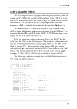
The following example program shows the initialization sequence
for the A/D-converter module ATD0 and a single-channel conversion
S12compact
16


