


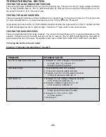


-35-
CIRCUIT DESCRIPTION
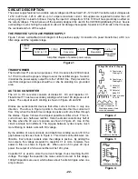
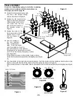
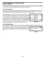
The function generator frequencies are produced by an XR2206
integrated circuit. This IC is capable of producing high quality sine,
square and triangle waveforms of high stability and accuracy. The
output waveform can be both amplitude and frequency modulated
by an external voltage. Figure P shows the block diagram of the
XR2206 IC.
The XR2206 is comprised of four functions blocks, a voltage con-
trolled oscillator (VCO), an analog multiplier and sine shaper, a
unity gain buffer amplifier, and a set of current switches.
The VCO actually produces an output frequency proportional to an
input current. Across pins 5 and 6, a timing capacitor is switched
in to give 5 different ranges of frequencies via COARSE FREQ
switch. On pin 7, the FINE FREQ ADJ variable resistor controls the
actual frequency output. These two components form the RC time constants for the oscillator frequency.
The VCO produces a square wave signal. This square wave is sent to a shaper and converted into a sine wave.
QUIZ - ANALOG SECTION
INSTRUCTIONS: Complete the following examination and check your answers carefully.
1. The analog multiplier is part of . . .
r
A. the voltage controlled oscillator.
r
B. unity gain buffer amplifier.
r
C. four function blocks.
r
D. timing capacitor circuit.
2. Increasing the current of the VCO will effect the . . .
r
A. amplitude.
r
B. DC offset.
r
C. AM modulation.
r
D. frequency.
3. The RC time constant is determined by . . .
r
A. pins 5 and 6.
r
B. voltage controlled oscillator.
r
C. pin 7 and a variable resistor.
r
D. components on pins 5, 6, and 7.
4. What pins on the 2206 IC are used to change the
sine wave to a saw wave?
r
A. 5, 6
r
B. 15, 16
r
C. 13, 14
r
D. 4, 12
5. Adjusting P4 from +12V to -12V effects . . .
r
A. sine wave amplitude.
r
B. modulation.
r
C. frequency stability.
r
D. DC offset.
6. Coarse frequency is set by . . .
r
A. P6.
r
B. capacitor C11 through C15.
r
C. C21.
r
D. P1 and SW9.
7. A 1 volt DC level on the FM input will . . .
r
A. shift the frequency 1kHz.
r
B. shift the frequency to DC.
r
C. have no effect.
r
D. shift the frequency 1MHz.
8. The square wave and CLK output are 180
o
out
of phase because . . .
r
A. Q2 inverts the CLK output.
r
B. Q1 inverts the square wave output.
r
C. a negative voltage is applied to P5.
r
D. pin 12 is tied to -12V.
9. Clipping of the sine wave outputs can be cor-
rected by . . .
r
A. P5.
r
B. the DC offset pot.
r
C. lowering the +5V power supply.
r
D. none of the above.
10. The sync output produces . . .
r
A. a sine wave.
r
B. a saw wave.
r
C. voltage spikes.
r
D. a square wave.
Functional Block Diagram
Figure P
1
16
2
15
3
14
4
13
5
12
6
11
7
10
8
9
Symmetry
ADJ.
Waveform
ADJ.
Ground
Sync
Output
Bypass
FKS
Input
Timing
Resistor
Timing
Capacitor
V+
Mult. Out
Sine/Saw
Output
AM Input
+1
Multiplier
and
Sine
Shaper
VCO
Current
Switches
Answer
s:
1.C;
2.D;
3.D;
4.C;
5.D;
6.B;
7.C;
8.A;
9.D;
10.D
Содержание XK-550K
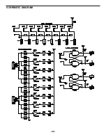
Страница 37: ...SCHEMATIC DIAGRAM ANALOG SECTION 36 ...
Страница 50: ...SCHEMATIC DIAGRAM 49 ...


