background image

CC1310 Wireless Module

E70 Series User Manual

Copyright ©2012–2017, Chengdu Ebyte Electronic Technology Co., Ltd.

12

/

34

3.2.2 Pin Definition

No.

Pin item

Pin direction

Application

1

GND

Ground

Ground electrode

2

ANT

Ground

Antenna (50Ω characteristic impedance)

4

NC

Reserved pin

Reserved, to be floated

5

NC

Reserved pin

Reserved, to be floated

6

LNA_EN

Output

Internal MCU controlled LNA pin, valid in high level, connect to pin 44

7

PA_EN

Output

Internal MCU controlled PA pin, valid in high level, connect to pin 45

8

NC

Reserved pin

Reserved, to be floated

9

NC

Reserved pin

Reserved, to be floated

10

NC

Reserved pin

Reserved, to be floated

11

NC

Reserved pin

Reserved, to be floated

12

NC

Reserved pin

Reserved, to be floated

13

NC

Reserved pin

Reserved, to be floated

14

NC

Reserved pin

Reserved, to be floated

15

M2

Input

M2, M1, M0 jointly decide the 8 working modes;

An external 1k protective resistor shall be connected in series when in use.

16

GND

Ground

Ground electrode

17

M1

Input

M2, M1, M0 jointly decide the 8 working modes;

An external 1k protective resistor shall be connected in series and a 1M pull-up resistor

shall be added when in use.

(Cannot be floated, it can be grounded when not used)

18

M0

Input

M2, M1, M0 jointly decide the 8 working modes;

An external 1k protective resistor shall be connected in series and a 1M pull-up resistor

shall be added when in use.

(Cannot be floated, it can be grounded when not used)

19

RXD

Input

TTL serial port input connecting to external TXD pin.

It can be configured as open-drain or

high pull input

, please refer to Parameter setting.

An external 1k protective resistor shall be

connected in series when in use.

20

TXD

Output

TTL serial port output connecting to external RXD input pin.

It can be configured as

open-drain or push-pull input

, please refer to Parameter setting.

An external 1k protective

resistor shall be connected in series when in use.

21

TMSC

Input

JTAG TMSC

22

TCKC

Input

JTAG TCKC

23

NC

Reserved pin

Reserved, to be floated

24

NC

Reserved pin

Reserved, to be floated

25

AUX

Output

It is used to indicate the operation status of module, for user to wake up the external MCU,

the module outputs low level during self-checking and initialization at power on,

it can be

configured as open-drain output or pull-up output,

please refer to parameter setting par.

An external 1k protective resistor shall be connected in series while using

(

can be floated)

26

VCC

-

Power positive reference,

Power supply 2.1V ~ 3.8V DC

Содержание E70 Series

Страница 1: ...roduct upgrade please refer to the latest version All rights to interpret and modify this manual belong to Chengdu Ebyte Electronic Technology Co Ltd Version Date Description Issued by 1 00 2017 11 06...

Страница 2: ...s are easily dropped The module has the function of data encryption compression The data of the module transmitted over the air features randomness And with the rigorous encryption decryption data int...

Страница 3: ...Pin Definition 12 3 3 E70 433T30S E70 868T30S E70 915T30S 13 3 3 1 Dimension 13 3 3 2 Pin Definition 14 4 Recommended Circuit Diagram 16 4 1 E70 433T14S2 E70 868T14S2 E70 915T14S2 16 4 2 General Circu...

Страница 4: ...4S2 E70 915T14S2 28 9 1 1 Secondary Development Dimension 28 9 1 2 The Pin Definition 28 9 2 E70 433T14S E70 868T14S E70 915T14S 29 9 2 1 Secondary Development Dimension 29 9 2 2 The Pin Definition 29...

Страница 5: ...efficiency good correction performance In case of sudden interference it can correct the interfered data packets proactively so that the reliability transmission range are improved correspondingly Wit...

Страница 6: ...14S CC1310 16 26 mm 1 65 0 1g 40 85 10 90 40 125 C E70 915T30S CC1310 24 38 5 mm 4 9 0 1g 40 85 10 90 40 125 C 2 2 Electrical Parameters 2 2 1 Transmitting Current Model Min Typ Max Unit Remarks E70 4...

Страница 7: ...umed by CPU RAM Clock and some registers which remain operating SoC is at very low power consumption status The turn off current is always lower than the current consumed when the power supply source...

Страница 8: ...ption can be lowered by lowering the transmitting power but the efficiency of the internal PA will be decreased by lowering transmitting power due to various reasons The transmitting power will be low...

Страница 9: ...907 0 915 0 922 5 MHz E70 915T30S 907 0 915 0 922 5 MHz 2 4 Tested Parameters Model Min Typ Max Unit Remarks E70 433T14S2 1350 1500 1600 m The external antenna used is of 2 5dBi gain and vertical pol...

Страница 10: ...evel to be floated 12 LNA_EN Output Internal MCU controlled LNA pin valid in high level to be floated 13 M2 Input M2 M1 M0 together decide the 8 kinds of working modes An external 1k protective resist...

Страница 11: ...nput please refer to Parameter setting An external 1k protective resistor shall be connected in series when in use 21 M1 Input M2 M1 M0 together decide the 8 kinds of working modes An external 1k prot...

Страница 12: ...when in use Cannot be floated it can be grounded when not used 18 M0 Input M2 M1 M0 jointly decide the 8 working modes An external 1k protective resistor shall be connected in series and a 1M pull up...

Страница 13: ...be floated 32 RESET Input Reset pin 33 NC Reserved pin Reserved to be floated 34 NC Reserved pin Reserved to be floated 35 NC Reserved pin Reserved to be floated 36 NC Reserved pin Reserved to be flo...

Страница 14: ...nnected in series when in use 17 GND Ground Ground electrode 18 M0 Input M2 M1 M0 jointly decide the 8 working modes An external 1k protective resistor shall be connected in series and a 1M pull up re...

Страница 15: ...floated 33 NC Reserved pin Reserved to be floated 34 NC Reserved pin Reserved to be floated 35 NC Reserved pin Reserved to be floated 36 NC Reserved pin Reserved to be floated 37 NC Reserved pin Reser...

Страница 16: ...y Co Ltd 16 34 4 Recommended Circuit Diagram 4 1 E70 433T14S2 E70 868T14S2 E70 915T14S2 4 2 General Circuit Diagram No Description STM8L MCU 1 The UART module is TTL level Please connect to MCU of TTL...

Страница 17: ...of module A as 0xFFFF or 0x0000 and the channel as 0x04 When module A is the transmitter transparent transmission all modules under channel 0x04 will receive the data the purpose of broadcast is reali...

Страница 18: ...d M0 Therefore the user needs to wait the AUX rising edge as the starting point of module s normal work 5 6 AUX Description 5 6 1 Indication of UART Output To wake up external MCU 5 6 2 Indication of...

Страница 19: ...0 UART opens Wireless closes and sub package transparent transmission is available Air data rate and baud rate can be adjusted separately It is applicable for data packet transmission 3 Configuration...

Страница 20: ...e when the transmitter works in mode 0 after the external MCU transmits data 12345 it can switch to sleep mode immediately without waiting the rising edge of the AUX pin also the user s main MCU will...

Страница 21: ...sses and baud rates must be same on both receiver and transmitter 4 In continuous mode both transmitter and receiver must be same model For example E70 868T14S and E70 868T30S cannot communicate in co...

Страница 22: ...tter can have different baud rate but same air data rate Advantage It can wake up the receiver under mode 6 wake up code will be added automatically before transmitting the code number depends on the...

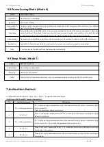
Страница 23: ...ly receive the data sent from the transmitter under mode 4 6 9 Sleep Mode Mode 7 Status M0 1 M1 1 M2 1 Transmitting Transmitting is not available Receiving Receiving is not available Others Other func...

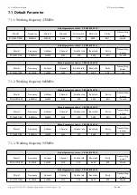
Страница 24: ...y 868MHz Default parameter values C0 00 00 18 4E 1C Model Frequency Address Channel Air data rate Baud rate Parity Transmitting power E70 868T14S2 868MHz 0x0000 0x0E 2 5K 9600 8N1 25mW Default paramet...

Страница 25: ...mode M0 1 M1 1 M2 0 User gives the module instruction HEX format C4 C4 C4 the module resets for one time During the reset process the module will conduct self check AUX outputs low level After reset c...

Страница 26: ...e can be used as high low address and channel The module changes its address and channel when transmitting And it will revert to original setting after the process is completed It is transparent trans...

Страница 27: ...power supply ripple is within 100mV Low power transmission is not recommended due to its low power supply efficiency 0 0 30dBm Default 0 1 27dBm 1 0 24dBm 1 1 21dBm For example The meaning of No 3 SPE...

Страница 28: ...6 DIO_9 Input Output MCU GPIO 7 DIO_8 Input Output MCU GPIO 8 VCC Positive power reference voltage range 2 2V 3 8V DC 9 GND Reference ground Ground electrode 10 GND Reference ground Ground electrode...

Страница 29: ...tz crystal with pin 4 4 X32K_Q2 Input Output Connect to 32 768K quartz crystal with pin 3 5 DIO_1 Input Output MCU GPIO 6 DIO_2 Input Output MCU GPIO 7 DIO_3 Input Output MCU GPIO 8 DIO_4 Input Output...

Страница 30: ...ut MCU GPIO 31 DIO_22 Input Output MCU GPIO 32 RESET Input Reset pin 33 DIO_23 Input Output MCU GPIO 34 DIO_24 Input Output MCU GPIO 35 DIO_25 Input Output MCU GPIO 36 DIO_26 Input Output MCU GPIO 37...

Страница 31: ...C Input JTAG TMSC 24 RESET Input Reset pin valid in low level 25 DIO_16 Input Output MCU GPIO 26 DIO_17 Input Output MCU GPIO 27 DIO_18 Input Output MCU GPIO 28 VCC Positive power reference voltage ra...

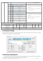
Страница 32: ...e more details in TI official document TDI and TDO pin can be unconnected Connection diagram of JTAG downloader 10 Production Guidance 10 1 Reflow Soldering Temperature Profile Feature Sn Pb Assembly...

Страница 33: ...ut in a metal case Power register was set incorrectly air data rate is set as too high the higher the air data rate the shorter the distance The power supply low voltage under room temperature is lowe...

Страница 34: ...his manual will be updated based on the upgrade of firmware and hardware please refer to the latest version Please refer to our website for new product information 13 About Us Technical support suppor...

Отзывы: