Diamond Systems DMM-16R-AT Скачать руководство пользователя страница 7


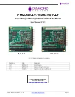
DMM-16R-AT  User Manual V1.31 

www.diamondsystems.com


Page 7


4.


BOARD CONFIGURATION 

Refer to the Drawing of DMM-16R-AT on Page 5 for locations of the configuration items mentioned here. 

4.1  I/O Base Address (ISA bus only) 

Each board in the system must have a different base address. In ISA bus mode, the board

’s base address is 

set  with  a  portion  of  jumper  block  J6,  located  at  the  lower  left  corner  of  the  board.  Each  of  the  six  jumper 
locations  marked  9,  8,  7,  6,  5,  4  corresponds  to  the  same-

numbered  address  bit  in  the  board’s  10-bit  I/O 

address. Bits 3-0 are always 0 for the base address, resulting in a 16-byte I/O address block. A jumper out is 
equal to a 1, and a jumper in is equal to a 0. Although any 16-byte location is selectable, certain locations are 
reserved  or  may  cause  conflicts  with  other  system  resources.  The  table  below  lists  recommended  base 
address settings for Diamond-MM-16R-AT. The default setting is 300 Hex. 


Base Address 

Jumper Position 

Hex 

Decimal 


220 

544 

Out 

In 

In 

In 

Out 

In 

240 

576 

Out 

In 

In 

Out 

In 

In 

250 

592 

Out 

In 

In 

Out 

In 

Out 

260 

608 

Out 

In 

In 

Out 

Out 

In 

280 

640 

Out 

In 

Out 

In 

In 

In 

290 

656 

Out 

In 

Out 

In 

In 

Out 

2A0 

672 

Out 

In 

Out 

In 

Out 

In 

2B0 

688 

Out 

In 

Out 

In 

Out 

Out 

2C0 

704 

Out 

In 

Out 

Out 

In 

In 

2D0 

720 

Out 

In 

Out 

Out 

In 

Out 

2E0 

736 

Out 

In 

Out 

Out 

Out 

In 

300 

768 (Default) 

Out 

Out 

In 

In 

In 

In 

330 

816 

Out 

Out 

In 

In 

Out 

Out 

340 

832 

Out 

Out 

In 

Out 

In 

In 

350 

848 

Out 

Out 

In 

Out 

In 

Out 

360 

864 

Out 

Out 

In 

Out 

Out 

In 

380 

896 

Out 

Out 

Out 

In 

In 

In 

390 

912 

Out 

Out 

Out 

In 

In 

Out 

3A0 

928 

Out 

Out 

Out 

In 

Out 

In 

3C0 

960 

Out 

Out 

Out 

Out 

In 

In 

3E0 

992 

Out 

Out 

Out 

Out 

Out 

In 


Содержание DMM-16R-AT

Страница 1: ...O PC 104 and PC 104 Plus Modules User Manual V1 31 DMM 16R AT DMM 16RP AT 2017 Diamond Systems Corporation FOR TECHNICAL SUPPORT PLEASE CONTACT support diamondsystems com Revision Date Comment 1 29 0...

Страница 2: ...ARD CONFIGURATION 7 6 I O REGISTER MAP 10 7 REGISTER DEFINITIONS 14 8 ANALOG INPUT RANGES AND RESOLUTION 27 9 PERFORMING AN A D CONVERSION 28 10 A D SCAN INTERRUPT AND FIFO OPERATION 31 11 ANALOG OUTP...

Страница 3: ...el DMM 16RP AT only NOTE For simplicity in this manual the term DMM 16R AT may be used to refer to both the PC 104 and the PC 104 Plus models of the board In instances where the information is specifi...

Страница 4: ...DMM 16R AT User Manual V1 31 www diamondsystems com Page 4 2 BLOCK DIAGRAMS Figure 1 DMM 16R AT Block Diagram Figure 2 DMM 16RP AT Block Diagram...

Страница 5: ...bus connector J3 User I O connector J4 A D single ended differential configuration jumper block J5 D A range and polarity configuration jumper block J6 DMA Interrupt Address configuration J7 Factory u...

Страница 6: ...els 7 0 in differential mode Vin 15 7 Vin 8 0 Analog input channels 15 8 in both single ended mode Low side of input channels 7 0 in differential mode Vout0 3 Analog output channels 0 3 Vref Out 5V pr...

Страница 7: ...byte location is selectable certain locations are reserved or may cause conflicts with other system resources The table below lists recommended base address settings for Diamond MM 16R AT The default...

Страница 8: ...e A single ended input uses 2 wires input and ground The measured input voltage is the difference between these two wires A differential input uses 3 wires input input and ground The measured input vo...

Страница 9: ...le behavior may result Both the range and polarity jumpers must be installed for proper analog output behavior 4 5 Interrupt Level Selection for ISA bus interface only Jumper block J6 is used to confi...

Страница 10: ...FO status register 11 Analog Configuration Register Analog and FIFO register readback Addresses 12 15 form a window into two 4 byte pages Addresses 10 15 constitutes the extended page of 6 bytes The p...

Страница 11: ...IFORST PAGE FIFOEN SCANEN CLKFRQ C2 C1 C0 11 SCNINT RANGE ADBU G1 G0 12 See next page 13 See next page 14 See next page 15 See next page READ operations 7 6 5 4 3 2 1 0 0 AD7 AD6 AD5 AD4 AD3 AD2 AD1 A...

Страница 12: ...tr1D3 Ctr1D2 Ctr1D1 Ctr1D0 14 Ctr2D7 Ctr2D6 Ctr2D5 Ctr2D4 Ctr2D3 Ctr2D2 Ctr2D1 Ctr2D0 15 SC1 SC0 RW1 RW0 M2 M1 M0 BCD Page 1 Page 1 is used to manage the autocalibration features WRITE operations Bit...

Страница 13: ...pages but they are different in read mode for page 2 Therefore they are included in the Read operation table below WRITE operations Bit no 7 6 5 4 3 2 1 0 12 A7 A6 A5 A4 A3 A2 A1 A0 13 B7 B6 B5 B4 B3...

Страница 14: ...ored and retrieved in interleaved fashion Data from the A D is put into the FIFO in little endian mode with the LSB inserted first and the MSB inserted second Thus the data comes out of the FIFO in th...

Страница 15: ...nge When the high channel is sampled the board resets to the low channel Base 3 Write Digital Output Port ISA Legacy mode Bit No 7 6 5 4 3 2 1 0 Name DIOB7 DIOB6 DIOB5 DIOB4 DIOB3 DIOB2 DIOB1 DIOB0 Wh...

Страница 16: ...D A channel must have its data written in the proper sequence First write the LSB to Base 1 then write the MSB to one of the MSB registers 4 7 depending on the D A selected Repeat these two writes for...

Страница 17: ...ted with PAGE bit CLRINT Clear interrupt request active only if EXTEN1 0 1 0 1 Clear interrupt request flip flop 0 No action Base 8 Read Status Register Bit No 7 6 5 4 3 2 1 0 Name STS TINT SD AINT AD...

Страница 18: ...would work only if Port A is input port Base 9 Read Control readback Bit No 7 6 5 4 3 2 1 0 Name AINTE EXTPG PAGE DMODE TINTE RSVD CLKEN CLKSEL This register may be used to read the values of various...

Страница 19: ...scans 0 Scan mode disabled the STS bit will remain high for a single conversion CLKFRQ Clock frequency for counter timer 1 0 10MHz 1 1MHz C2 External Clock Gate Enable 1 IN0 pin 29 on the I O header...

Страница 20: ...and PAGE reads back as 0 However its register contents are preserved so that later when EXTPG returns to 0 the page returns to its previous setting of 0 or 1 FIFOEN Readback of FIFOEN bit described o...

Страница 21: ...RANGE ADBU A D full scale range 0 0 5V 0 1 Invalid setting 1 0 10V 1 1 0 10V G1 0 A D gain setting G1 G0 Gain 0 0 1 0 1 2 1 0 4 1 1 8 The gain setting is the ratio between the A D full scale range sho...

Страница 22: ...gister Bit No 7 6 5 4 3 2 1 0 Name Ctr1D7 Ctr1D6 Ctr1D5 Ctr1D4 Ctr1D3 Ctr1D2 Ctr1D1 Ctr1D0 Base 14 Read Write Counter 2 Data register Bit No 7 6 5 4 3 2 1 0 Name Ctr2D7 Ctr2D6 Ctr2D5 Ctr2D4 Ctr2D3 Ctr...

Страница 23: ...D3 D2 D1 D0 D7 0 Calibration data to be read or written to the EEPROM and or TrimDAC During EEPROM or TrimDAC write operations the data written to this register will be written to the selected device...

Страница 24: ...et to 0 When CMUXEN 0 P_MUXEN1 0 should be set to 1 TDACEN TrimDAC Enable Writing 1 to this bit will initiate a transfer to the TrimDAC used in the auto calibration process Base 14 Read Calibration St...

Страница 25: ...O port A data When DIO Enhanced mode is selected this register is used to read write data to port A Alternate Functions see Counter Timer Operation Chapter A0 External A D trigger A2 Counter 0 Gate In...

Страница 26: ...e FIFO contents are preserved and no new data will be written to the FIFO To clear an overflow condition the FIFO must be reset with the FIFORST bit in register 10 FF FIFO full flag set to 0 when the...

Страница 27: ...ound and the board will measure the difference between the voltages of the two inputs Polarity is important for a differential input Diamond MM 16R AT will subtract the voltage on the low input from t...

Страница 28: ...re to perform A D conversions on a group of consecutively numbered channels you do not need to write the input channel prior to each conversion For example to read from channels 0 2 write Hex 20 to ba...

Страница 29: ...n the status register at Base 8 When the A D converter is busy performing an A D conversion this bit is 1 and when the A D converter is idle conversion is done and data is available this bit is 0 Here...

Страница 30: ...A D value 32768 Full scale input range Example Input range is 5V and A D value is 17761 Input voltage 17761 32768 5V 2 710V For a bipolar input range 1 LSB 1 32768 Full scale voltage Here is an illust...

Страница 31: ...s low 0 0 1 A D scans are triggered by write to B 0 All channels between LOW and HIGH will be sampled STS stays high during the entire scan multiple A D conversions No interrupt occurs The user progra...

Страница 32: ...The resolution is the smallest possible change in output voltage For a 12 bit DAC the resolution is 1 2 12 or 1 4096 of the full scale output range This smallest change results from an increase or dec...

Страница 33: ...Output voltage symbolic formula Output voltage for 0 5V range 0 0V 0 0000V 1 1 LSB VREF 4096 0 0012V 2047 VREF 2 1 LSB 2 4988V 2048 VREF 2 2 5000V 2049 VREF 2 1 LSB 2 5012V 4095 VREF 1 LSB 4 9988V Con...

Страница 34: ...the full scale reference voltage 11 2 Write the value to the selected output channel The four DACs share a single address for the LSB Base 1 Each DAC then has its own MSB address Writing to the DAC s...

Страница 35: ...at the factory and stored in the EEPROM During calibration the average offset is added to the measured output of DAC 0 and this value is used as the comparison value to minimize overall errors During...

Страница 36: ...no Jumper on Pins 9 10 DIO Enhanced mode In Legacy mode the DIO ports are accessed at Base 3 To access port B outputs simply write an 8 bit value to base 3 Similarly to read the port A inputs read fr...

Страница 37: ...e counter 0 external clock input are configured for the same direction Note that this setting also affects the default value for DIO A2 counter 0 gate and DIO A0 counter 1 2 gate when these pins are n...

Страница 38: ...value and decrements by 1 each time a clock edge appears at the input The number of input clocks can be determined by reading the current count register and subtracting it from the original value On...

Страница 39: ...ic Reference Voltage 5 000V 3mV 5mA max output current Digital I O No of IOs 16 HCT TTL compatible 3 3V 5V jumper configurable Input voltage 5V operation Logic 0 0 0V min 1 65V max Logic 1 3 35V min 5...

Отзывы: