


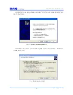
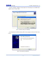


PCIe-AIO14 User Manual (Rev 1.2)
- 18 -
http://www.daqsystem.com
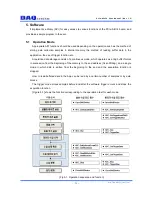
7
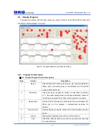
Ch. Value
The selected channel value is represented by HEX. Bit 0 is set
to "CH0" and bit 15 is set to "CH15". Since "CH0" selection is
AIN0, AIN1 is selected, and "CH15" selection is AIN30 and
AIN31 because channel selection is for two ADCs.
8
Ch. Counts
Number of selected channels. A channel twice as many as the
7th bit set number is selected.
9
Sampling Rate
(10~2Msps)
Set the ADC data sampling frequency (SPS). The setting range
is a maximum of 2,000,000 (2Msps) at a minimum of 10sps, and
decreases by a multiple of the set value according to the number
of channel selections. See Section 5.4.6.
10
Samples
Samples per channel
11
Blocks
The data block having the number of samples of the selected
channel data
12
Buffer Size
The buffer size is calculated by the input buffer variable. Buffer
Size = number of channels (8 times) x number of samples (10) x
number of data blocks (11).
13
Read Length
The number of samples read from the API when reading
collected data.
14
WR Ptr.
Buffer write pointer
15
RD Ptr.
Buffer read pointer
16
Sample/sec
Number of samples per second per channel block
17
Save
Open the file in folder 19, file name.
18
…
Folder search and file name selection, input
19
“C:\\data.txt”
Storage path and file name, selected in 18, the file path entered
is displayed. The default path is "C: \\ data.txt".
20
Single Buf/
Continuous Buf
Select the storage buffering method of the acquisition sample of
the normal mode measurement. Single mode, continuous mode.
21
Start/Stop
Start the normal mode data collection with the 'Start' button.
Buffering that does not support the trigger function collects data
from the device inside the library, and the application periodically
reads the data of the library and displays it on the graph.
Reading method is different according to 20 buffering method.
22
ReadEn
Read control data from the library buffer. Read data in the check
state and display it on the graph.
23
Run
Checks if a trigger has occurred on the selected channel and
reads and stops the status if it occurs. When the trigger occurs,