background image


PCIe-AIO14 User Manual (Rev 1.2) 


- 17 - 


http://www.daqsystem.com
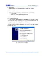
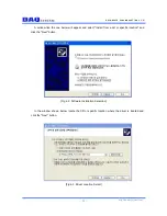
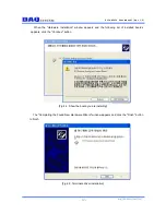
 

5.4     Sample Program 

It  implements  a  library  (API)  for  easy  access  to various  functions  of  the  PCIe-AIO14  board,  and 

provides a sample program to the user. 

3

4

1

2

5

6

7

8

9

11
12

10

13

14
15
16

17

18

19

20

21

22

23

24

25

26

27

28

29

30

31

32

33

34

35

36
37
38

39

40

41

42

43

44

45

46

47

48


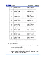
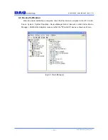
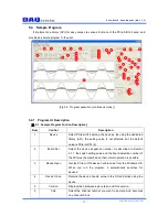
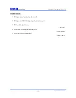
[Fig 5-2. Program execution (continuous mode)] 


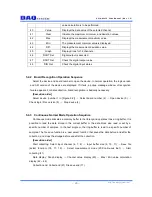
5.4.1  Program UI Description 

[

  5-1. Sample Program Fuction Description] 

Num 

Control 

Description 

Device 

Select  PCIe-AIO14  among  the  devices.  By  using  the  dedicated 

library  (API),  the  setting  value  is  not  affected,  but  the  default 

value is PCIe-AIO14 (4). 

Board Sel. 

Select  the  device  sequence  number.  As  described  in  Section 

3.1.1, the switch setting value and the board selection number of 

the API must be matched so that normal operation is possible. 

Device Open 

Get the PCIe-AIO14 device handle value from the Windows OS. 

When  you  run  the  program,  it  automatically  searches  for 

devices. 

Device Close 

Returns the device handle  value to the OS and stops using the 

device. 

Version 

Displays the hardware logic version and DLL version. 

CHx 

Select  the  channel  number  you  want  to  sample.  And  becomes 

one channel block. 

Содержание PCIe-AIO14

Страница 1: ...Q system is believed to be accurate and reliable However no responsibility is assumed by DAQ system for its use nor for any infringements of patents or other rights of third parties which may result f...

Страница 2: ...dware 3 1 Board Switch Setup 3 2 I O Connector J1 J2 3 3 Digital I O Connector J8 3 4 Analog Signal MUX 3 5 Digital I O 4 Installation 4 1 Confirm Contents 4 2 Installation Sequence 4 3 Device Verific...

Страница 3: ...analog signal multiplex input for each ADC 10V Differential Signal input Level 10 2Msps Variable Sampling Setup 32 Ch Software Trigger 24 Bit Digital Input Output Input output shielding by photo coup...

Страница 4: ...input for each ADC Resolution 16 bit Sampling Rate 10 2Msps 1 Channel Signal Type Differential Digital I O Bit Inpit 24 Bit Output 24 Bit Isolator Photo Coupler TLP291 4 or Compatible Input Signal 12...

Страница 5: ...nnector description and board installation 3 1 Board Switch Setup Explain the jumper and switch selection on the board J7 J1 J2 Fig 3 1 Connector Switch Layout 3 1 1 Board Number Setup Switch J7 It is...

Страница 6: ...r compatible product Table 3 1 J1 Connector Description Pin Description Pin Description 1 Reserved 35 Reserved 2 Analog Ground AGND 36 Reserved 3 30 Input AINN30 37 Analog Ground AGND 4 30 Input AINP3...

Страница 7: ...alog Ground AGND 34 0 Input AINP0 68 Reserved Please inquire about the availability of analog input cable and terminal block board when you purchase the product 3 2 2 Connector J2 The 16 bit analog di...

Страница 8: ...ut AINP9 60 Digital Ground GND 27 7 Input AINN7 61 Analog Ground AGND 28 7 Input AINP7 62 Digital Ground GND 29 5 Input AINN5 63 Analog Ground AGND 30 5 Input AINP5 64 Digital Ground GND 31 3 Input AI...

Страница 9: ...tal Input DIN18 12 Digital Input DIN19 13 Digital Input DIN20 14 Digital Input DIN21 15 Digital Input DIN22 16 Digital Input DIN23 17 Digital Input DIN_COM2 18 Digital Ground GND 19 Digital Ground GND...

Страница 10: ...l MUX When one channel block is composed of a plurality of data channel selections the interchannel acquisition interval is a maximum sampling rate of 2Msps supported by the chip and the interval betw...

Страница 11: ...he DIN_COM pin and the HI input signal is input to the DIN signal the internal signal becomes LO to sense the signal input DIN0 BIN0 BINx 3 3V 3 3V 2 4K DINx 2 4K DIN_COM Fig 3 6 Digital Input Circuit...

Страница 12: ...Installation CD Driver Manual API Sample Program etc 4 2 Installation Sequence The board should be used in Windows XP SP2 over Windows 7 Windows 8 and Windows 10 First turn off the PC insert the PCIe...

Страница 13: ...elow will appear and select Install from a list or specific location and click the Next button Fig 4 2 Software Installation Selection In the window shown below locate the CD or specific location wher...

Страница 14: ...allation window appears and the following list of installed boards appears click the Continue button Fig 4 4 Show the board you are installing The Completing the Found New Hardware Wizard window appea...

Страница 15: ...hen the board installation is complete check that the device is assigned to the OS Control Panel System System Properties Device Manager Select Execute in order Under Device Manager Multifunction Adap...

Страница 16: ...function etc Acquisition data storage consists of a continuous mode which operates as a ring buffer format in succession from the beginning of the memory to the end address Over Writing and a single...

Страница 17: ...variables Start data collection and create a data memory buffer 5 2 4 Checking the measurement status ADC_GetBufferedCount ADC_GetBlockState Number of data buffering samples in continuous mode read wr...

Страница 18: ...d trigger motion control 5 3 4 Start measurement ADC_Run ADC_TriggerRun Initialize logic variables start data acquisition and data memory buffers and start trigger operation 5 3 5 Checking the Trigger...

Страница 19: ...CIe AIO14 among the devices By using the dedicated library API the setting value is not affected but the default value is PCIe AIO14 4 2 Board Sel Select the device sequence number As described in Sec...

Страница 20: ...h The number of samples read from the API when reading collected data 14 WR Ptr Buffer write pointer 15 RD Ptr Buffer read pointer 16 Sample sec Number of samples per second per channel block 17 Save...

Страница 21: ...les per channel is the product of Samples and the number of channels that set the trigger variable 31 Set Sets the number of trigger acquisition samples 32 State Read the trigger status value It is di...

Страница 22: ...oard recognition is basically necessary Execution order Select device number 1 in Figure 5 2 Select board number 2 Open device 3 Check logic DLL version 5 Stop device 4 5 4 3 Continuous Normal Mode Op...

Страница 23: ...7 5 4 5 Trigger Mode Operation Sequence Data collection execution performs continuous or single mode memory buffering Execute trigger operation for the selected channel to save and stop sample data wh...

Страница 24: ...ollowing figure If more than one channel is selected the time interval to the adjacent channel is the ADC highest sampling rate 2Msps and the interval between channel blocks maintains the time of the...

Страница 25: ...om References 1 PCI Express Base Specification Revision 2 0 2 PCI Exprss to PCI PCI X Bridge Specification Revision 1 0 3 PCI Local Bus Specification PCI SIG 4 AN201 How to build application using API...

Отзывы: