8
DS726PP2
CS4525
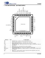
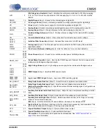
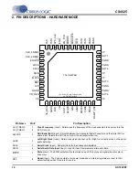
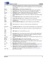
1. PIN DESCRIPTIONS - SOFTWARE MODE
Pin Name
Pin #
Pin Description
INT
1
Interrupt
(Output
) - Indicates an interrupt condition has occurred.
SCL
2
Serial Control Port Clock
(
Input
) - Serial clock for the I²C control port.
SDA
3
Serial Control Data
(
Input/Output
) -
Bi-directional data I/O for the I²C control port.
LRCK
4
Left Right Clock
(
Input
) - Determines which channel, Left or Right, is currently active on the serial
audio data line.
SCLK
5
Serial Clock
(
Input
)
-
Serial bit clock for the serial audio interface.
SDIN
6
Serial Audio Data Input
(
Input
) - Input for two’s complement serial audio data.
HP_DETECT/
MUTE
7
Headphone Detect / Mute
(
Input
) - Headphone detection or mute input signal as configured via the
I²C control port.
RST
8
Reset
(
Input
) - The device enters a low power mode and all internal registers are reset to their
default settings when this pin is driven low.
Top-Down (Through Package) View
48-Pin QFN Package
12
7
6
5
4
3
2
1
11
10
9
8
25
30
31
32
33
34
35
36
26
27
28
29
14
13
15
16
17
18
19
20
21
22
23
24
47
48
46
45
44
43
42
41
40
39
38
37
INT
SCL
SDA
LRCK
SCLK
SDIN
HP_DETECT/MUTE
RST
LVD
DGND
VD_REG
VD
VP
OUT1
PGND
PGND
OUT2
VP
VP
OUT3
PGND
PGND
OUT4
VP
VA
_
R
E
G
AGN
D
FI
L
T
+
VQ
AFIL
TL
AF
IL
TR
AINL
AIN
R
OC
REF
PGND
PGND
RAMP_C
AP
XTI
XT
O
SYS_CLK
AUX
_
LRCK/AD0
AUX
_
SCLK
AUX
_
SDOUT
DL
Y_SDIN/EX_TWR
DL
Y_SDOUT
PWM_SIG1
PWM_SIG2
PGND
PGND
Thermal Pad


