background image

CRD5378

DS639RD2

47

3.5.6

Customize

The 

Customize

 sub-panel sends commands to upload custom FIR and IIR filter coefficients, upload cus-

tom test bit stream data, start the digital filter, stop the digital filter, and write/read custom EEPROM con-
figuration files to the on-board boot EEPROM. Example data files are included in a sub-directory of the
software installation.

3.5.7

External Macros

Macros are generated within the 

Macros

 sub-panel on the 

Control

 panel. Once a macro has been built

it can either be saved with a unique macro name to be run within the 

Macros

 sub-panel, or saved as an

external macro and be associated with one of the 

External Macro

 buttons.

A macro is saved as an 

External Macro

 by saving it in the 

. /macros/

 subdirectory using the name

‘m1.mac’

‘m2.mac’

, etc. Depending on the selected name the macro will be associated with the corre-

sponding 

External Macro

 button 

M1

M2

, etc.

• M1 = . /macros/m1.mac

• M2 = . /macros/m2.mac

• etc.

External Macro

 buttons can be re-named on the panel by right clicking on them. The button name will

change, but the macro associated with that button is always saved as 

‘m1.mac’

‘m2.mac’

, etc., in the

. /macros/

 subdirectory. The 

External Macro

 button names are stored in the file 

‘Mnames.txt’

, also in the

. /macros/

 subdirectory.

External Macro

s allow up to eight macros to be accessed quickly without having to load them into the 

Mac-

ros

 sub-panel on the 

Control

 panel. These 

External Macro

s operate independently of the 

Macros

 sub-

panel and are not affected by operations within it, except when a macro is saved to the 

. /macros/

 subdi-

rectory to replace a currently existing 

External Macro

.

Control

Description

Load FIR Coef

Write a set of FIR coefficients into the digital filter from a file.

Load IIR Coef

Write a set of IIR coefficients into the digital filter from a file.

Load TBS Data

Write a set of test bit stream data into the digital filter from a file.

Start Filter

Enables the digital filter by sending the 

Start Filter

 command.

Stop Filter

Disables the digital filter by sending the 

Stop Filter

 command.

Control

Description

M1 - M8

Runs the 

External Macro

 associated with that button.

Содержание CRD5378

Страница 1: ...single channel seismic chip set Data sheets for the CS3302A CS5373A and CS5378 devic es should be consulted when using the CRD5378 reference design Pin headers connect an external differential sensor to the analog inputs of the measurement channel An on board test DAC creates precision differential analog sig nals for in circuit performance testing without an external signal source The reference d...

Страница 2: ...CRD5378 2 DS639RD2 REVISION HISTORY Revision Date Changes RD1 JAN 2007 Initial release RD2 JAN 2008 Upgrade from CS3302 to CS3302A ISZ G U19 Change R27 R28 R29 R30 from 0ohms to 680ohms ...

Страница 3: ... Cirrus integrated circuits or other products of Cirrus This consent does not extend to other copying such as copying for general distribution advertising or promotional purposes or for creating any work for resale CERTAIN APPLICATIONS USING SEMICONDUCTOR PRODUCTS MAY INVOLVE POTENTIAL RISKS OF DEATH PERSONAL INJURY OR SEVERE PROP ERTY OR ENVIRONMENTAL DAMAGE CRITICAL APPLICATIONS CIRRUS PRODUCTS ...

Страница 4: ...4 Delta Sigma Test DAC 18 2 2 5 Voltage Reference 18 2 3 Digital Hardware 19 2 3 1 Digital Filter 19 2 3 2 Microcontroller 22 2 3 3 RS 485 Telemetry 24 2 3 4 UART Connection 26 2 3 5 External Connector 27 2 4 Power Supplies 27 2 4 1 Analog Voltage Regulators 27 2 5 PCB Layout 28 2 5 1 Layer Stack 28 2 5 2 Differential Pairs 28 2 5 3 Bypass Capacitors 30 3 SOFTWARE DESCRIPTION 31 3 1 Menu Bar 31 3 ...

Страница 5: ...gure 1 CRD5378 Block Diagram 12 Figure 2 Differential Pair Routing 29 Figure 3 Quad Group Routing 29 Figure 4 Bypass Capacitor Placement 30 LIST OF TABLES Table 1 Amplifier Pin 13 Jumper Setting 7 Table 2 System Clock Input Setting 7 Table 3 CS5378 PLL Mode Select Setting R15 R41 R42 7 Table 4 Input SYNC Source Selection Setting 7 Table 5 CS5378 SYNC Source Selection Setting 7 Table 6 Pin Header I...

Страница 6: ...dows 2000 or Windows XP with an available USB port Internet access to download the evaluation software 1 2 Hardware Setup To set up the CRD5378 reference design hardware Verify all jumpers are in the default settings see next section With power off connect the CRD5378 power inputs to the power supply outputs J26 pin 17 3 3 V J26 pin 19 3 3 V J26 pin 20 0 V Connect the USB cable between the CRD5378...

Страница 7: ...e 2 System Clock Input Setting Digital Filter Clock Resistor 4 096 MHz Manchester R15 R41 R42 2 048 MHz Manchester R42 1 024 MHz Manchester R41 32 768 MHz R41 R42 4 096 MHz R15 2 048 MHz R15 R42 1 024 MHz R15 R41 32 768 MHz Not Populated Table 3 CS5378 PLL Mode Select Setting R15 R41 R42 Sync Source Jumper RS 485 R47 R48 Direct Output R49 R50 R45 Table 4 Input SYNC Source Selection Setting Sync So...

Страница 8: ... stallation application will automatically be created Open the Volume1 sub folder and run setup exe If the Seismic Evaluation Software has been pre viously installed the uninstall wizard will automatically remove the previous version during install Follow the instructions presented by the Cirrus Seismic Evaluation Installation Wizard The default in stallation location is C Program Files Cirrus Sei...

Страница 9: ... Evaluation GUI Installation Guide is available from the Cirrus Logic web site with step by step instructions on installing the USBXpress driver 1 3 4 Launching the Seismic Evaluation Software Important For reliable USB communication the USBXpress driver must be installed after the Seismic Evaluation Software installation but before launching the application The USBXpress driver files are in clude...

Страница 10: ...aunch the evaluation software and apply power to CRD5378 Click OK on the About panel to get to the Setup panel On the Setup panel select Open Target on the USB Port sub panel When connected the Board Name and MCU code version will be displayed 1 4 1 Noise Test Noise performance of the measurement channel can be tested as follows Set the controls on the Setup panel to match the picture ...

Страница 11: ...oise statistics Verify the noise performance S N is 124 dB or better 1 4 2 Distortion Test Set the controls on the Setup panel to match the picture Once the Setup panel is set select Configure on the Digital Filter sub panel After digital filter configuration is complete click Capture on the Data Capture sub panel Once the data record is collected the Analysis panel is automatically displayed Sele...

Страница 12: ...m Major blocks of the CRD5378 reference design include CS3302A Hydrophone Amplifier CS5373A Σ Modulator Test DAC CS5378 Digital Filter PLL Precision Voltage Reference Microcontroller with USB RS 485 Transceivers Voltage Regulators Figure 1 CRD5378 Block Diagram ...

Страница 13: ...shield The CS3301A geophone amplifier does not have a GUARD output Instead the CS3301A amplifier expects an MCLK clock input to pin 13 which is needed for its chopper stabilization circuitry When using a CS3301A amplifier a cable shield termination to GND is pro vided for the sensor connection By default CRD5378 uses the CS3302A amplifier Therefore the GUARD signal is connected to pin 3 of the inp...

Страница 14: ...lt in ESD protection diodes guaranteed to 2000 V HBM 200 V MM JEDEC standard The small physical size of these ESD diodes restricts their current capacity to 10 mA For land applications that use the CS3301A amplifier the INA input has a common mode and differential RC filter The common mode filter sets a low pass corner to shunt very high frequency components to ground with minimal noise contributi...

Страница 15: ...the selected sensor which are available from the sensor manufacturer Land Common Mode Filter Specification Value Common Mode Capacitance 10 nF 10 Common Mode Resistance 200 Ω Common Mode 3 dB Corner 6 dB octave 80 kHz 10 Land Differential Filter Specification Value Differential Capacitance 10 nF 10 Differential Resistance 200 Ω 200 Ω 400 Ω Differential 3 dB Corner 6 dB octave 40 kHz 10 Marine Comm...

Страница 16: ...ut pin 13 In order to run the chopper circuitry synchronous to the modulator analog sampling clock the CS3301A amplifier pin 13 connects to the CS5378 digital filter MCLK CRD5378 can be converted to use either the CS3301A and CS3302A amplifiers by installing the amplifier device and populating R8 R9 and R10 with 0 Ω resistors accordingly Replacement amplifiers can be requested as samples from the ...

Страница 17: ...es resistors and a differential anti alias RC filter is created by connecting 20 nF of high linearity differential capacitance 2x 10 nF C0G between each half of the rough and fine signals 2 2 3 Delta Sigma Modulator The CS5373A Σ modulator performs the A D function for differential analog signals from the CS3301A 02A amplifier The digital output from the modulator is an oversampled Σ bit stream 2 ...

Страница 18: ...quirements specified in the CS5373A data sheet 2 2 5 Voltage Reference A voltage reference on CRD5378 creates a precision voltage from the regulated analog supplies for the modulator and test DAC VREF inputs Because the voltage reference output is generated relative to the negative analog power supply VREF is near GND potential for bipolar power supplies Analog Signals Description OUT Precision di...

Страница 19: ...so creates a Σ bit stream output to create analog test signals in the CS5373A test DAC The CS5378 requires several control signal inputs from the external system Configuration and data collection are through the SPI port Modulator Σ data is input through the modulator interface and test DAC Σ data is generated by the test bit stream generator Control Signals Description RESETz Reset input active l...

Страница 20: ...about the PLL input clock and BOOT mode selections at reset can be found in the CS5378 data sheet 2 3 1 2 Configuration SPI Port On CRD5378 configuration of the digital filter is through the SPI port by the on board 8051 microcontrol ler which receives commands from the PC evaluation software via the USB interface Evaluation software commands can write read digital filter registers specify digital...

Страница 21: ...ecification Value Input Clock Frequency 1 024 2 048 4 096 MHz Distributed Clock Synchronization 240 ns Maximum Input Clock Jitter RMS 1 ns Specification Value PLL Internal Clock Frequency 32 768 MHz Maximum Jitter RMS 300 ps Loop Filter Architecture Internal Specification Value Oscillator Citizen 32 768 MHz VCXO CSX750VBEL32 768MTR Surface Mount Package Type Leadless 6 Pin 5x7 mm Supply Voltage Cu...

Страница 22: ... 32 pin LQFP package 9mm x 9mm Industrial temperature full performance including USB from 40 C to 85 C Internal temperature sensor with range violation interrupt capability Internal timers four general purpose plus one extended capability Power on reset can supply a reset signal to external devices Analog ADC 10 bit 200 ksps SAR with internal voltage reference Analog comparators arbitrary high low...

Страница 23: ...unused in CRD5378 14 P2 4 MODE2 CS5373A mode control 15 P2 3 MODE1 CS5373A mode control 16 P2 2 MODE0 CS5373A mode control Pin Pin Name Assignment Description 17 P2 1 GPIO General Purpose I O unused in CRD5378 18 P2 0 GPIO General Purpose I O CS5378 RESETz 19 P1 7 BYP_EN I2C bypass switch control 20 P1 6 SDA_DE I2C data driver enable 21 P1 5 SCL I2C clock in out 22 P1 4 SDA I2C data in out 23 P1 3...

Страница 24: ...By default the C8051F320 microcontroller uses an internally generated 12 MHz clock for compatibility with USB standards 2 3 2 5 Timebreak Signal By default the C8051F320 microcontroller sends the TIMEB signal to the digital filter for the first collected sample of a data record By default 100 initial samples are skipped during data collection to ensure the CS5378 digital filters are fully settled ...

Страница 25: ... signal must be synchronized to the network at the transmitter since no local timing adjustment is available A microcontroller hardware connection is made when the SYNC_IO signal is received over the dedicated RS 485 twisted pair and detected by a microcontroller interrupt The microcontroller can then use an in ternal counter to re time the SYNC signal output to the digital filter SYNC input as re...

Страница 26: ...depending how the telemetry system is to be implemented Dynamic address assignment uses daisy chained I2C connections to assign an address to each mea surement node Once a node receives an address it enables the I2 C bypass switches to the next node so it can be assigned an address Static address assignment has a serial number assigned to each node during manufacturing When placed in the network t...

Страница 27: ...and to help settle transients and another 0 01 uF capacitor to bypass high frequency noise 2 4 1 Analog Voltage Regulators Linear voltage regulators create the positive and negative analog power supply voltages to the analog components on CRD5378 These regulate the 3 3 V and 3 3 V power supply inputs to create the 2 5 V and 2 5 V analog power supplies Pins Name Signal 1 2 CLK CLK Clock Input 3 4 S...

Страница 28: ... analog signals on CRD5378 are differentially routed CRD5378 layer 3 is dedicated for power supply routing Each power supply net includes at least 68 µF bulk capacitance as a charge well for settling transient currents CRD5378 layer 4 is dedicated as a digital routing layer CRD5378 layer 5 is a solid ground plane without splits or routing A solid ground plane provides the best return path for bypa...

Страница 29: ...2 wire IN and IN differential pairs and are routed as such Analog signal connections out of the CS3301A 02A amplifiers and into the CS5372 modulators are 4 wire INR INF INF INR quad groups and are routed with INF and INF as a tra ditional differential pair and INR and INR as guard traces outside the respective INF and INF traces Figure 2 Differential Pair Routing INA INA INA INA Figure 3 Quad Grou...

Страница 30: ...ly pin includes 0 1 µF bypass capacitors placed as close as possible to the pin Each power supply net includes at least 68 µF bulk capacitance as a charge well for transient current loads Figure 4 Bypass Capacitor Placement VD Bypass CS3302A Device VA bypass VA bypass ...

Страница 31: ...clipboard Print Analysis Screen Prints the full Analysis panel including statistics fields Print Analysis Graph Prints only the graph from the Analysis panel High Resolution Printing Prints using the higher resolution of the printer Low Resolution Printing Prints using the standard resolution of the screen Quit Exits the application software Setup Displays the Setup Panel Analysis Displays the Ana...

Страница 32: ...8 32 DS639RD2 3 2 About Panel The About panel displays copyright information for the Cirrus Seismic Evaluation software Click OK to exit this panel Select Help Ö About from the menu bar to display this panel ...

Страница 33: ...anel The Setup panel initializes the evaluation system to perform data acquisition It consists of the following sub panels and controls USB Port Digital Filter Analog Front End Test Bit Stream Gain Offset Data Capture External Macros ...

Страница 34: ...tup Analysis and Control panel access becomes unavailable in the menu bar The evaluation software constantly monitors the USB connection status and automatically disconnects if the target board is turned off or the USB cable is unplugged Board Name Displays the type of target board currently connected MCU code version Displays the version number of the microcontroller code on the connected target ...

Страница 35: ... SPS 0 25 mS to 1 S are available Output Filter Selects the output filter stage from the digital filter Sinc output FIR1 output FIR2 output IIR 1st order output IIR 2nd order output or IIR 3rd order output can be selected FIR2 output provides full decimation of the modulator data FIR Coeff Selects the on chip FIR coefficient set to use in the digital filter Linear phase or min imum phase FIR coeff...

Страница 36: ...tion external INA inputs or external INB inputs can be selected DAC Mode Selects the operational mode of the CS5373A test DAC The test DAC operational modes are AC dual output OUT BUF AC precision output OUT only AC buffered output BUF only DC common mode output DC Common DC differential output DC Diff or AC common mode output AC Common The test DAC can also be powered down PWDN when not in use to...

Страница 37: ...libration results are automatically written to the OFFSET registers and remain there even after offset calibration is disabled Control Description Gain Displays the digital filter GAIN1 to GAIN4 registers Offset Displays the digital filter OFFSET1 to OFFSET4 registers Read Reads values from the GAIN and OFFSET registers Write Writes values to the GAIN and OFFSET registers USEGR Enables gain correc...

Страница 38: ...e type of analysis windowing function to be applied to the collected data set Used to ensure proper analysis of discontinuous data sets Bandwidth Limit Hz Sets the frequency range over which to perform analysis used to exclude higher fre quency components Default value of zero performs analysis for the full Nyquist fre quency range Full Scale Code Defines the maximum positive full scale 24 bit cod...

Страница 39: ...macros m2 mac etc External Macro buttons can be re named on the panel by right clicking on them The button name will change but the macro associated with that button is always saved as m1 mac m2 mac etc in the macros subdirectory The External Macro button names are stored in the file Mnames txt also in the macros subdirectory External Macros allow up to eight macros to be accessed quickly without ...

Страница 40: ... 3 4 Analysis Panel The Analysis panel is used to display the analysis results on collected data It consists of the following controls Test Select Statistics Plot Enable Cursor Zoom Refresh Harmonics Spot Noise Plot Error ...

Страница 41: ...nd then plots sample occur rence vs sample value Only valid for noise data since sine wave data varies over too many codes to plot as a histogram Signal FFT Runs an FFT on the collected data set and then plots frequency magnitude vs fre quency Statistics are calculated using the largest frequency bin as a full scale signal reference Noise FFT Runs an FFT on the collected data set and then plots fr...

Страница 42: ...e Cursor will snap to the closest plotted point and the plot values for that point display below the graph Control Description Time Domain Max Maximum code of collected data set Min Minimum code of collected data set Histogram Max Maximum code of collected data set Min Minimum code of collected data set Mean Mean of collected data set Std Dev Standard Deviation of collected data set Variance Varia...

Страница 43: ... fundamental and harmonic bins used to calculate the Signal FFT statistics HARMONICS highlighting helps to understand the source of any Signal FFT plot errors 3 4 7 Spot Noise The Spot Noise control labeled dB or nV is only visible during a Noise FFT analysis and selects the units used for plotting the graph either dB Hz or nV Hz The dB Hz plot applies the Full Scale Code value from the Data Captu...

Страница 44: ... Panel The Control panel is used to write and read register settings and to send commands to the digital filter It consists of the following sub panels and controls DF Registers DF Commands SPI1 Macros GPIO Customize External Macros ...

Страница 45: ...er Control Description Address Selects a digital filter register Data Contains the data written to or read from the register Read Initiates a register read Write Initiates a register write Control Description Command Selects the command to be written to the digital filter Write Data 1 Contains the SPI1DAT1 data to be written to the digital filter Write Data 2 Contains the SPI1DAT2 data to be writt...

Страница 46: ...lects special commands that can be performed Data Sets the register data value for the inserted macro command Also sets the parame ter value for special commands Clear Clears the currently displayed macro Load Loads a previously saved macro Save Saves the currently displayed macro Macros can be saved with unique names or can be saved as External Macros Insert Inserts a macro command at the selecte...

Страница 47: ...ons can be re named on the panel by right clicking on them The button name will change but the macro associated with that button is always saved as m1 mac m2 mac etc in the macros subdirectory The External Macro button names are stored in the file Mnames txt also in the macros subdirectory External Macros allow up to eight macros to be accessed quickly without having to load them into the Mac ros ...

Страница 48: ... RES 0603 DO NOT POPULATE 21 020 01095 Z1 A RES 4 99k OHM 1 10W 1 NPb 0603 1 R5 DALE CRCW06034K99FKEA 22 020 01128 Z1 A RES 9 53k OHM 1 10W 1 NPb 0603 1 R6 DALE CRCW06039K53FKEA 23 020 01130 Z1 A RES 10k OHM 1 10W 1 NPb 0603 FILM 1 R7 DALE CRCW060310K0FKEA 24 020 00673 Z1 A RES 0 OHM 1 10W 5 NPb 0603 FILM 16 R10 R24 R34 R36 R43 R44 R46 R47 R48 R52 R53 R54 R57 R59 R62 R71 DALE CRCW0603000Z0EA ECO55...

Страница 49: ...CRD5378 DS639RD2 49 5 LAYER PLOTS ...

Страница 50: ...CRD5378 50 DS639RD2 ...

Страница 51: ...CRD5378 DS639RD2 51 ...

Страница 52: ...CRD5378 52 DS639RD2 ...

Страница 53: ...CRD5378 DS639RD2 53 ...

Страница 54: ...CRD5378 54 DS639RD2 ...

Страница 55: ...CRD5378 DS639RD2 55 ...

Страница 56: ...CRD5378 56 DS639RD2 ...

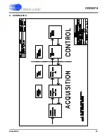
Страница 57: ...CRD5378 DS639RD2 57 6 SCHEMATICS ...

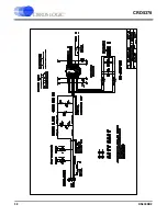
Страница 58: ...CRD5378 58 DS639RD2 ...

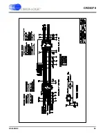
Страница 59: ...CRD5378 DS639RD2 59 ...

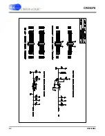
Страница 60: ...CRD5378 60 DS639RD2 ...

Страница 61: ...CRD5378 DS639RD2 61 ...

Страница 62: ...CRD5378 62 DS639RD2 ...

Страница 63: ...CRD5378 DS639RD2 63 ...

Страница 64: ...CRD5378 64 DS639RD2 ...

Отзывы: