background image

www.balluff.com

83

english

7.8.3  Variant Dependence
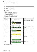
2 – AdSS

Length

Value

Description

20

0x0030 (48)

0x0031 (49)

0x4000 (16384)

0x8004 (32772)

0x8006 (32774)

0x8007 (32775)

0x8008 (32776)

0x8009 (32777)

BLOB_Transfer

FirmwareUpdate

Identification_Diagnosis

TeachChannel

Adjustable Switching Data Channel

TeachIn Single Value

TeachIn Two Value

TeachIn Dynamic

Tab. 7-29:  Variant dependence: 2 – AdSS
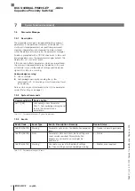
3 – LSSC

Length

Value

Description

22

0x0001 (1)

0x0030 (48)

0x0031 (49)

0x4000 (16384)

0x8001 (32768)

0x8004 (32772)

0x8007 (32775)

0x8008 (32776)

0x8009 (32777)

SSP_Legacy

BLOB_Transfer

FirmwareUpdate

Identification_Diagnosis

Switching Signal Channel

TeachChannel

TeachIn Single Value

TeachIn Two Value

TeachIn Dynamic

Tab. 7-30:  Variant dependence: 3 – LSSC

4 – CM

Length

Value

Description

22

0x0001 (1)

0x0030 (48)

0x0031 (49)

0x4000 (16384)

0x8001 (32768)

0x8004 (32772)

0x8007 (32775)

0x8008 (32776)

0x8009 (32777)

SSP_Legacy

BLOB_Transfer

FirmwareUpdate

Identification_Diagnosis

Switching Signal Channel

TeachChannel

TeachIn Single Value

TeachIn Two Value

TeachIn Dynamic

Tab. 7-31:  Variant dependence: 3 – CM

7


System Functions (continued)

BCS  Q40BBAA-PIM20C-EP _ _ _ -GS04

Capacitive Proximity Switches

Содержание BCS Q40BBAA-PIM20C-EP-GS04 Series

Страница 1: ...BCS Q40BBAA PIM20C EP___ GS04 deutsch Konfigurationsanleitung english Configuration Guide...

Страница 2: ...www balluff com...

Страница 3: ...BCS Q40BBAA PIM20C EP___ GS04 Konfigurationsanleitung deutsch...

Страница 4: ...www balluff com...

Страница 5: ...ationsdaten 12 3 5 System Commands 21 3 6 Events 22 4 Kommunikationsparameter 24 5 Prim re Ger tefunktionen 25 5 1 Identifikation Identification 25 5 2 Ger teerkennung Device Discovery 26 5 3 N herung...

Страница 6: ...2 7 4 Variantenkonfiguration Variant Configuration 73 7 5 Pinzuweisung Pin Assignment 75 7 6 Bedeutung der LED Zust nde und Konfiguration LED Meaning and Configuration 78 7 7 Prozessdateninformation u...

Страница 7: ...Symbole und Konventionen Einzelne Handlungsanweisungen werden durch ein vorangestelltes Dreieck angezeigt Handlungsanweisung 1 Handlungsabfolgen werden nummeriert dargestellt 1 Handlungsanweisung 1 2...

Страница 8: ...hrieben 2 Basiswissen IO Link 2 5 Prozessdatenstrom Die Daten bertragung basiert auf der allgemeinen Profil spezifikation IO Link Common Profile 1 0 Beispiel siehe Bild 2 1 Bild 2 1 Byte 0 7 0 39 30 B...

Страница 9: ...ch Daten gewollt ver ndern oder Down loads wenn z B ein falsch parametriertes Ger t ange schlossen wird Das System aus Master und Device stellt so einen Ger teaustausch ohne die Notwendigkeit einer ak...

Страница 10: ...toring siehe Seite 62 Status extremer Umweltbedingung Extreme Environ ment Status siehe Seite 64 Interne Temperatur Internal Temperature siehe Seite 66 3 1 3 Systemfunktionen Ger testatus und detailie...

Страница 11: ...en schaltenden Sensor nach Smart Sensor Profil Ed 1 Die Prozessdaten enthalten vier Schaltsignale LSSC1 4 sowie weitere Statussignale Device ID Baudrate PDInput PDOutput IO Link Protokoll version Mini...

Страница 12: ...cer Signal Byte 2 Bit 7 MSB Bit 6 Bit 5 Bit 4 Bit 3 Bit 2 Bit 1 Bit 0 LSB System Error Reserved SSC4 LSSC4 SSC3 LSSC3 SSC2 LSSC2 SSC1 LSSC1 Tab 3 5 Prozessdatenprofil PDInput LSSC 3 3 3 PDInput CM Byt...

Страница 13: ...SB Device Temperature Byte 11 12 Bit 7 MSB Bit 6 Bit 5 Bit 4 Bit 3 Bit 2 Bit 1 Bit 0 Reserved Byte 13 Byte 14 Bit 7 MSB Bit 6 Bit 5 Bit 4 Bit 3 Bit 2 Bit 1 Bit 0 Bit 7 Bit 6 Bit 5 Bit 4 Bit 3 Bit 2 Bi...

Страница 14: ...Firmware Revision 0x0017 23 0 R 10 Byte STRING n a Application Specific Tag 0x0018 24 0 R W 32 Byte STRING Ja Function Tag 0x0019 25 0 R W 32 Byte STRING Ja Location Tag 0x001A 26 0 R W 32 Byte STRING...

Страница 15: ...R W 1 Byte UINT8 Nein 0x01 Switchpoint Hysteresis 3 R W 2 Byte INT16 Nein 0x0F 15 1 5 Fine Adjust Config 0x0056 86 0 R W 2 Byte Nein Channel 1 R W 1 Byte UINT8 Nein 0x00 Mode 2 R W 1 Byte UINT8 Nein 0...

Страница 16: ...ein 0 Signal Delay On Delay 0x0098 152 0 R W 8 Byte Ja Channel 1 1 R W 2 Byte UINT16 Nein 0 Channel 2 2 R W 2 Byte UINT16 Nein 0 Channel 3 3 R W 2 Byte UINT16 Nein 0 Channel 4 4 R W 2 Byte UINT16 Nein...

Страница 17: ...2 Byte UINT16 Nein 85 Channel 2 2 R W 2 Byte UINT16 Nein 85 Channel 3 3 R W 2 Byte UINT16 Nein 85 Channel 4 4 R W 2 Byte UINT16 Nein 85 Speed Lower Limit High 0x0534 1332 0 R W 8 Byte Ja Channel 1 1...

Страница 18: ...NT8 ENUM Nein 0 Switch Counter Limit 0x02F2 754 0 R W 8 Byte Ja Channel 1 1 R W 2 Byte UINT16 Nein 2 Channel 2 2 R W 2 Byte UINT16 Nein 2 Channel 3 3 R W 2 Byte UINT16 Nein 2 Channel 4 4 R W 2 Byte UI...

Страница 19: ...2 0x0077 119 0 R W 8 Byte Ja Logic Block 1 Input 2 1 R W 2 Byte UINT16 Nein 0 Logic Block 2 Input 2 2 R W 2 Byte UINT16 Nein 0 Logic Block 3 Input 2 3 R W 2 Byte UINT16 Nein 0 Logic Block 4 Input 2 4...

Страница 20: ...1 R W 4 Byte FLOAT32 Nein immer als 0 gelesen und akzeptiert Upper Threshold Temperature 2 R W 2 Byte INT16 Nein 90 Lower Threshold Temperature 3 R W 2 Byte INT16 Nein 25 Lifetime Extreme Status 0x00...

Страница 21: ...R W 1 Byte UINT8 ENUM Ja 0 Event Code Suppression 0x0071 113 0 R W 10 Byte Ja Event Code Suppression 1 5 R W 2 Byte UINT16 Nein 0 Event Code Suppression Teach in 0x0072 114 0 W 2 Byte UINT16 n a Even...

Страница 22: ...UM Nein 3 Digital Input Pin 2 Digital Configuration 0x0094 148 0 R W 4 Byte Ja Signal Source 1 R W 2 Byte UINT16 ENUM Nein 0x003E 62 Teach in Logic 2 R W 1 Byte UINT8 ENUM Nein 0 Normal Type 3 R W 1 B...

Страница 23: ...ird abgebrochen die Setpoints werden auf die Voreinstellungen Default zur ckgesetzt 0x4F 79 Teach Cancel Der Teach in Vorgang wird abgebrochen 0x80 128 Device Reset F hrt einen Warmstart des Ger ts du...

Страница 24: ...peed Monitoring pr fen 0 Device is operating properly 0x8CB8 36024 Warnung Einer der Speed Monitoring Kan le hat die obere Grenze berschritten Speed Monitoring pr fen 0 Device is operating properly 0x...

Страница 25: ...n 0 Device is operating properly 0x8D23 36131 Fehler Schreibzyklenlimit erreicht Speichern nicht mehr gew hrleistet Austausch empfohlen 1 Maintenance Required 0x8D24 36132 Warnung Parameterschreibfehl...

Страница 26: ...1 Kommunikationsparameter Um die grundlegenden Kommunikationsparameter flexibel an die Anwendung anzupassen k nnen auch andere Ger tevarianten eingestellt werden siehe Tab 4 2 auf Seite 24 Folgende Ge...

Страница 27: ...PIM20C EP00 3 GS04 Product Order Code 0x0701 1793 0 R 7 Byte STRING n a z B BCS01AJ Tab 5 1 Identifikation ISDU Application Specific Tag Mit dem Parameter Application Specific Tag kann ein String max...

Страница 28: ...DU Device Discovery Timeout Der Parameter Device Discovery Timout stellt die Zeitdauer des Device Discovery Signals ein das ber LEDs ange zeigt wird Der Wert wird in Minuten angegeben Es ist der Werte...

Страница 29: ...lue wird in der Funktion Schaltprofile Switching Profiles verwendet um bin re Schaltsignale zu erhalten Die Schaltsignale k nnen ber Schaltausg nge als Schaltsignale ausgegeben werden ber IO Link als...

Страница 30: ...4 0x7FFFFFFC Tab 5 5 Schaltprofile Schaltpunktauswertung deaktivieren 5 Prim re Ger tefunktionen Fortsetzung bersicht AdSS Profil Nur ein Schaltkanal Switching Signal Channel SSC verf gbar Nur ein Sch...

Страница 31: ...kt 2 50 der eingestellten Hyste rese oder der Messwert ist gr er gleich Schaltpunkt 1 50 der eingestellten Hysterese so schaltet der Ausgang inaktiv Bild 5 6 High SP1 SP2 Hyst Hyst Low Messwert Schalt...

Страница 32: ...TP2 Low Workflow 1 Teach SP1 TP1 2 Teach SP1 TP2 3 Teach Apply Messwert Schaltausgang Two Value Teach im Single Point Mode 5 Prim re Ger tefunktionen Fortsetzung Bild 5 10 High SP1 TP1 TP1 TP2 TP2 SP2...

Страница 33: ...her am Sensor Mit dem Befehl Fine Adjust far wird der Schaltpunkt aus Richtung des Sensors angepasst d h der neue Schaltpunkt ist weiter vom Sensor entfernt Abh ngig vom gew hlten Schaltprofil vom Sch...

Страница 34: ...High SP1 SP2 Low Messwert Schaltausgang 1 nur f r LSSC Profil Tab 5 6 Fine Adjustment Coupled Adjustment Mode AdSS und LSSC Profil Setpoint 1 Adjustment Mode nur f r LSSC Profil Der Modus Setpoint 1 A...

Страница 35: ...vorgang wird durch die Anzeige Teach In dargestellt gr n gelbe LED wechselt langsam Leuchtet die gr ne LED dauerhaft Anzeige Ready oder Communication ist der Teachvorgang erfolgreich been det Der Sens...

Страница 36: ...ess Data 5 4 4 ISDU AdSS Name Index Subindex Zugriff L nge Datentyp Data Storage Default SSC Parameter SP 0x0038 56 0 R W 16 Bit INT16 Ja 0x0000 0 SSC Configuration Logic 0x0039 57 0 R W 8 Bit UINT8 J...

Страница 37: ...0 Teachpoint nicht erfasst oder nicht erfolgreich erfasst 4 Flag SP TP1 1 Teachpoint erfolgreich erfasst 3 0 State 0 IDLE Kein aktuell aktiver Teachvorgang 1 SUCCESS Letzter Vorgang war erfolgreich 2...

Страница 38: ...Nein 0x01 Switchpoint Hysteresis 3 R W 2 Byte INT16 Nein 0x0F 15 1 5 Fine Adjust Config 0x0056 86 0 R W 2 Byte Nein Channel 1 R W 1 Byte UINT8 Nein 0x00 Mode 2 R W 1 Byte UINT8 Nein 0x00 SSC 3 Paramet...

Страница 39: ...1 war erfolgreich 2 SP2 SUCCESS Letzter Vorgang f r SP2 war erfolgreich 3 SP12 SUCCESS Letz ter Vorgang f r SP1 und SP2 war erfolgreich 4 WAIT FOR COMMAND Warte auf n chstes Kommando 5 BUSY Vorgang ak...

Страница 40: ...l deaktiviert 0x01 1 Single Point Einzelpunktmodus SP1 aktiviert 0x02 2 Window Schaltbereichsmodus SP1 SP2 aktiviert 0x03 3 Two Point Zweipunktmodus SP1 SP2 aktiviert Switchpoint Hysteresis 0x000A 0x0...

Страница 41: ...in f r Setpoint 21 0x4A 74 Teach SP2 Stop Stoppt dyna misches Teach in f r Setpoint 2 und berechne den Schaltpunkt1 0x4E 78 Teach Reset Der Teach in Vor gang wird abgebrochen die Set points werden auf...

Страница 42: ...atik Algorithmus Bild 6 1 Signalverz gerung Mathematik Algorithmus 6 1 3 Process Data Object ID Name Beschreibung Richtung 0x0008 8 Signal Delay Channel 1 Ausgangssignal Signal Delay Channel 1 Eingang...

Страница 43: ...Channel 4 4 R W 1 Byte UINT8 ENUM Nein 0 Signal Delay On Delay 0x0098 152 0 R W 8 Byte Ja Channel 1 1 R W 2 Byte UINT16 Nein 0 Channel 2 2 R W 2 Byte UINT16 Nein 0 Channel 3 3 R W 2 Byte UINT16 Nein 0...

Страница 44: ...Teach In Teach In 0x0041 65 Lifetime Extreme Eine oder mehrere Extembedingungen liegen vor 0x004E 78 Temperature Status Customer Limits Ger tetemperatur au erhalb des eingestellten Tempera turbereichs...

Страница 45: ...nn die Zeit f r Aus Verz gerung und One Shot eingestellt werden Der Wert stellt die Zeit in Millisekunden dar Der Wertebereich liegt zwischen 0x0000 0 und 0xFFFF 65535 Ein Wert von 0x0000 0 stellt kei...

Страница 46: ...ory Settings Setzt beschreibbare Parameter auf den Defaultwert zur ck Tab 6 6 Signalverz gerung System Commands F r eine bersicht aller System Commands siehe Kapi tel 3 5 auf Seite 21 6 1 6 Variantena...

Страница 47: ...g Speed Ok Channel 4 Switching Speed Value Channel 4 innerhalb der Grenzen Eingang 0x00C7 199 Switching Speed Value Channel 1 Switching Speed Value Channel 1 Eingang 0x00C8 200 Switching Speed Value C...

Страница 48: ...in 85 Channel 2 2 R W 2 Byte UINT16 Nein 85 Channel 3 3 R W 2 Byte UINT16 Nein 85 Channel 4 4 R W 2 Byte UINT16 Nein 85 Speed Lower Limit High 0x0534 1332 0 R W 8 Byte Ja Channel 1 1 R W 2 Byte UINT16...

Страница 49: ...de kann der aktuelle Modus der Z hlfunktion ausgew hlt werden Wert Bedeutung Beschreibung 0x00 0 Deactivated deaktiviert 0x01 1 Speed Geschwindigkeits berwachung Tab 6 9 Signalgeschwindigkeits berwach...

Страница 50: ...tartver z gerung dar Speed Monitoring State Mit Speed Monitoring State kann der aktuelle Status abgelesen werden Wert Bedeutung Beschreibung 0x00 0 Idle Es liegt noch kein Geschwin digkeitswert vor 0x...

Страница 51: ...Application Reset Setzt beschreibbare Parameter auf den Defaultwert zur ck 0x82 130 Restore Factory Settings Setzt beschreibbare Parameter auf den Defaultwert zur ck Tab 6 12 Signalgeschwindigkeits be...

Страница 52: ...he Bild 6 3 Ist der Z hlerwert kleiner als die konfigurierte Z hlergrenze wird das Z hlerzustandsflag not reached gesetzt Sobald der Z hlwert gr er oder gleich der konfigurierten Z hler grenze ist wir...

Страница 53: ...s Z hlerzustandsflag not reached gesetzt Sobald der Z hlwert gr er oder gleich der konfigurierten Z hler grenze ist wird das Z hlerzustandsflag reached gesetzt Ist der Z hlwert gr er als die konfiguri...

Страница 54: ...el 1 Switching Counter Value Channel 1 Eingang 0x008D 141 Switching Counter Value Channel 2 Switching Counter Value Channel 2 Eingang 0x008E 142 Switching Counter Value Channel 3 Switching Counter Val...

Страница 55: ...0x02F3 755 0 R W 4 Byte Ja Channel 1 1 R W 1 Byte UINT8 ENUM Nein 0 Channel 2 2 R W 1 Byte UINT8 ENUM Nein 0 Channel 3 3 R W 1 Byte UINT8 ENUM Nein 0 Channel 4 4 R W 1 Byte UINT8 ENUM Nein 0 Switchin...

Страница 56: ...Zeit in Sekunden dar Der Wertebereich liegt zwischen 0x00 0 und 0xFF 255 Ein Wert von 0x00 0 stellt keine Startverz gerung dar 6 Sekund re Ger tefunktionen Fortsetzung Switching Counter State Mit Swit...

Страница 57: ...ter pr fen 0 Device is operating properly 0x8D19 36121 Warnung Einer der Switching Counter Kan le hat den maximalen Z hlstand erreicht Switching Counter pr fen 0 Device is operating properly Tab 6 21...

Страница 58: ...n des Logikblock Modus und die Eingangssig nale k nnen ber ISDU Parameterzugriff eingestellt wer den Obwohl jeder Logikblock 4 Eing nge unterst tzt kann ein Block mit weniger Eing ngen verwendet werde...

Страница 59: ...dex 3 INPUTS Logik Block 3 RESULT Index 0x76 Subindex 4 INPUTS Logik Block 4 RESULT Index 0x77 Subindex 3 Index 0x77 Subindex 4 Index 0x7A Subindex 3 Index 0x7A Subindex 4 Index 0x78 Subindex 3 Index...

Страница 60: ...ogic Block 4 Input 1 4 R W 2 Byte UINT16 Nein 0 Logic Block Input 2 0x0077 119 0 R W 8 Byte Ja Logic Block 1 Input 2 1 R W 2 Byte UINT16 Nein 0 Logic Block 2 Input 2 2 R W 2 Byte UINT16 Nein 0 Logic B...

Страница 61: ...Beginnend mit einer Speicherung nach 1 Minute danach 2 Minuten danach 4 Minuten danach 8 Minuten bis zu einem maximalen Speicherintervall von 12 Minuten 6 5 3 Process Data Object ID Name Beschreibung...

Страница 62: ...nach jedem Speichervorgang Dies ist auf ein Speicherintervall von 12 Minuten begrenzt Die Intervalle betragen 1 2 4 8 12 Minuten 0x01 1 Static Betriebsstundenz hler werden alle 12 Minuten gespeichert...

Страница 63: ...2 n a Custom Boot Cycle Counter 2 R 4 Byte UINT32 n a Tab 6 31 Betriebsstartz hler ISDU Die maximale Anzahl von Speicherzyklen betr gt 1 000 000 und bedeutet bei einer An und Abschaltung alle 12 Minut...

Страница 64: ...oder Kurzschluss an Pin 2 erkannt Eingang 0x0017 23 Undervoltage TRUE das Spannungsniveau liegt unter dem Schwellenwert Eingang 0x0018 24 Overvoltage TRUE das Spannungsniveau liegt ber dem Schwellenwe...

Страница 65: ...evice Status 0x5110 20752 Warnung berschreitung der prim ren Versorgungsspannung Abweichungen in der Versorgung pr fen 2 Out of Specification 0x5111 20753 Warnung Unterschreitung der prim ren Versorgu...

Страница 66: ...der Zeitz hler einen Fehler von maximal 180 Sekunden haben 6 8 3 Process Data Object ID Name Beschreibung Richtung 0x0041 65 Lifetime Extreme Eine oder mehrere Extrembedingungen liegen vor Eingang 0x...

Страница 67: ...eschreibung 1 Upper Temperature Die Temperatur liegt oberhalb des Schwellenwerts 2 Lower Temperature Die Temperatur liegt unterhalb des Schwellenwerts Tab 6 39 Status extremer Umweltbedingung State Ti...

Страница 68: ...gestellten Kun denlimits Index 0x0053 Gesetzt wenn au erhalb der Limits Eingang 0x004F 79 Temperature Status Device Limits Temperaturstatus Warnung bezogen auf die Ger telimits Gesetzt wenn au erhalb...

Страница 69: ...pezifischen Temperaturgrenzen betrie ben Gefahr von Ger tesch den 4 Failure 0x4210 16912 Warnung Device Temperature Overrun Clear Heat Of Source Gefahr von Ger teschaden Das Ger t ist zu hei Hitzequel...

Страница 70: ...er im Ger t vorliegt Diese Information ist gekoppelt mit dem Device Status 4 Failure der durch verschiedene Ger tefunktionen bzw Diagnose meldungen ausgel st werden kann Sobald der Fehlerzustand nicht...

Страница 71: ...e Neukonfiguration Zur cksetzen auf Werkseinstellungen kann weiterhelfen Sonst muss der Balluff Service kontaktiert oder das Ger t ausge tauscht werden Tab 7 3 Device Status 7 1 5 Detailed Device Stat...

Страница 72: ...NT16 Nein 0 Event Code Suppression Teach in 0x0072 114 0 W 2 Byte UINT16 n a Event Code Suppression Delete 0x0073 115 0 W 2 Byte UINT16 n a Tab 7 5 Diagnoseunterdr ckung ISDU 7 2 3 Diagnosis Level Con...

Страница 73: ...wert und wird als FREE interpretiert Jede Event Meldung ist wie folgt aufgebaut Byte1 MSB Byte0 LSB Event Code High Byte Event Code Low Byte Tab 7 7 Diagnoseunterdr ckung Event Message Suppression Eve...

Страница 74: ...chgef hrt R cksetzen aller Parameter und Ger teeinstellungen auf Standardwerte mit Ausnahme der Identifikations und Tagging Parameter Keine R cksetzung der Konfiguration der Ger tevariante DS Upload A...

Страница 75: ...Parameter umstellen oder durch Verwendung des IO Link Kompatibit tsmodus Wenn dieser Parameter beschrieben wird wird nicht sofort die Ger tevariante ge ndert sondern erst nach einem Neustart des Ger t...

Страница 76: ...ntenkonfiguration ISDU Device Variant Der Parameter zeigt an welche Ger tevariante aktuell eingestellt ist Folgende Ger tevarianten sind verf gbar Wert Bedeutung Beschreibung 2 AdSS Adjustable Switchi...

Страница 77: ...nk 1 R W 1 Byte UINT8 ENUM Nein 0 Mode 2 R W 1 Byte UINT8 ENUM Nein 1 Digital Output Pin 4 Digital Configuration1 0x0091 145 0 R W 4 Byte Ja Signal Source 1 R W 2 Byte UINT16 ENUM Nein 0x0038 56 ADSS1...

Страница 78: ...Mit Signal Source kann die interne Signalquelle f r den Pin ausgew hlt werden Es stehen verschiedene Signalquellen zur Verf gung die auf einem Pin ausgegeben oder einge lesen werden k nnen Wert Name...

Страница 79: ...ng Logic Type Mit Type kann der Ausgang konfiguriert werden Wenn Mode 0 Eingang ist den Type auf 0 setzen Wert Name Beschreibung Digital 0x00 0 PNP PNP Ausgang 0x01 1 NPN NPN Ausgang 0x02 2 Push Pull...

Страница 80: ...Pin 2 Pin 4 Gr n schnell blinkend Kurzschluss an Pin 2 oder Pin 4 Failure 100 ms 100 ms 100 ms 100 ms 100 ms 100 ms 100 ms 100 ms 100 ms 100 ms GN YE Allgemeiner Fehler Teach in No Object Das Ger t b...

Страница 81: ...ung zu ber cksichtigen 7 7 2 ISDU Name Index Sub index Zugriff L nge Datentyp Data Storage Default Process Data Profile selection 0x0051 81 0 R W 1 Byte UINT8 ENUM Ja AdSS 2 LSSC 3 CM 4 Process Data I...

Страница 82: ...Daten Data Type Type Lenght Bit Offset Beschreibung AdSS 1 3 01 01 00 1 Set of BoolT 1 0 Schaltsignal ADSS1 4 6 01 01 07 1 Set of BoolT 1 7 System Error LSSC 1 3 01 04 00 1 Set of BoolT 4 0 Schaltsig...

Страница 83: ...iese Vari ante nicht g ltig ist wird das Defaultprofil f r die entspre chende Variante ausgew hlt Event Code Event Typ Event Beschreibung Abhilfe Device Status 0x1850 6224 Benach richti gung Process D...

Страница 84: ...e Profil ID angegeben bedeutet das dass alle enthaltenen Funktionsklassen unterst tzt werden Falls nur Teilfunktionen spezifiziert sind werden diese explizit als einzelne Funktionsklasse ausgegeben Di...

Страница 85: ...0x8004 32772 0x8007 32775 0x8008 32776 0x8009 32777 SSP_Legacy BLOB_Transfer FirmwareUpdate Identification_Diagnosis Switching Signal Channel TeachChannel TeachIn Single Value TeachIn Two Value TeachI...

Страница 86: ...ands 0xC1 Acknowledge User Parameters Reset an das Ger t best tigen Daten k nnen ber den IO Link Parameterserver Data Storage siehe Seite 7 sehr einfach wiederhergestellt werden 7 9 2 System Commands...

Страница 87: ...BCS Q40BBAA PIM20C EP___ GS04 Configuration Guide english...

Страница 88: ...www balluff com...

Страница 89: ...and Functions 8 3 1 Overview of the included Functions 8 3 2 Device Variants 9 3 3 Process Data Profiles 10 3 4 ISDU Identification Data 12 3 5 System Commands 21 3 6 Events 22 4 Communication parame...

Страница 90: ...nosis Suppression 70 7 3 Reset Commands 72 7 4 Variant Configuration 73 7 5 Pin Assignment 75 7 6 LED Meaning and Configuration 78 7 7 Process Data Info and Configuration 79 7 8 Profile Characteristic...

Страница 91: ...ate this document 1 2 Symbols and conventions Individual instructions are indicated by a preceding triangle Instruction 1 Action sequences are numbered 1 Instruction 1 2 Instruction 2 Numbers not othe...

Страница 92: ...meters are described in chapter 4 on page 24 2 IO Link Basic Knowledge 2 5 Process Data Flow The data transfer is based on the general profile specification IO Link Common Profile 1 0 see Fig 2 1 for...

Страница 93: ...zation data of a device on the master The master controls the process between uploads if data is intentionally changed or downloads if e g an incorrectly parameterized device is connected The system c...

Страница 94: ...see page 61 Voltage and Current Monitoring see page 62 Extreme Environment Status see page 64 Internal Temperature see page 66 3 1 3 System Functions Device Status and Detailed Device Status see page...

Страница 95: ...Smart Sensor Profile Ed 1 The process data contains four switching signals LSSC1 4 as well as additional status signals Device ID Baud rate PDInput PDOutput IO Link protocol version Minimum cycle tim...

Страница 96: ...7 MSB Bit 6 Bit 5 Bit 4 Bit 3 Bit 2 Bit 1 Bit 0 LSB System Error Reserved SSC4 LSSC4 SSC3 LSSC3 SSC2 LSSC2 SSC1 LSSC1 Tab 3 5 Process data profile PDInput LSSC 3 3 3 PDInput CM Byte 0 Byte 1 Bit 7 MSB...

Страница 97: ...B Device Temperature Byte 11 12 Bit 7 MSB Bit 6 Bit 5 Bit 4 Bit 3 Bit 2 Bit 1 Bit 0 Reserved Byte 13 Byte 14 Bit 7 MSB Bit 6 Bit 5 Bit 4 Bit 3 Bit 2 Bit 1 Bit 0 Bit 7 Bit 6 Bit 5 Bit 4 Bit 3 Bit 2 Bit...

Страница 98: ...evision 0x0017 23 0 R 10 Bytes STRING n a Application Specific Tag 0x0018 24 0 R W 32 Bytes STRING Yes Function Tag 0x0019 25 0 R W 32 Bytes STRING Yes Location Tag 0x001A 26 0 R W 32 Bytes STRING Yes...

Страница 99: ...Mode 2 R W 1 Byte UINT8 No 0x01 Switchpoint Hysteresis 3 R W 2 Bytes INT16 No 0x0F 15 1 5 Fine Adjust Config 0x0056 86 0 R W 2 Bytes No Channel 1 R W 1 Byte UINT8 No 0x00 Mode 2 R W 1 Byte UINT8 No 0...

Страница 100: ...0 Signal Delay On Delay 0x0098 152 0 R W 8 Bytes Yes Channel 1 1 R W 2 Bytes UINT16 No 0 Channel 2 2 R W 2 Bytes UINT16 No 0 Channel 3 3 R W 2 Bytes UINT16 No 0 Channel 4 4 R W 2 Bytes UINT16 No 0 Sig...

Страница 101: ...W 2 Bytes UINT16 No 85 Channel 2 2 R W 2 Bytes UINT16 No 85 Channel 3 3 R W 2 Bytes UINT16 No 85 Channel 4 4 R W 2 Bytes UINT16 No 85 Speed Lower Limit High 0x0534 1332 0 R W 8 Bytes Yes Channel 1 1...

Страница 102: ...1 Byte UINT8 ENUM No 0 Switch Counter Limit 0x02F2 754 0 R W 8 Bytes Yes Channel 1 1 R W 2 Bytes UINT16 No 2 Channel 2 2 R W 2 Bytes UINT16 No 2 Channel 3 3 R W 2 Bytes UINT16 No 2 Channel 4 4 R W 2 B...

Страница 103: ...77 119 0 R W 8 Bytes Yes Logic Block 1 Input 2 1 R W 2 Bytes UINT16 No 0 Logic Block 2 Input 2 2 R W 2 Bytes UINT16 No 0 Logic Block 3 Input 2 3 R W 2 Bytes UINT16 No 0 Logic Block 4 Input 2 4 R W 2 B...

Страница 104: ...ion 1 R W 4 Bytes FLOAT32 No Always read and accepted as 0 Upper Threshold Temperature 2 R W 2 Bytes INT16 No 90 Lower Threshold Temperature 3 R W 2 Bytes INT16 No 25 Lifetime Extreme Status 0x00D1 20...

Страница 105: ...W 1 Byte UINT8 ENUM Yes 0 Event Code Suppression 0x0071 113 0 R W 10 Bytes Yes Event Code Suppression 1 5 R W 2 Bytes UINT16 No 0 Event Code Suppression Teach in 0x0072 114 0 W 2 Bytes UINT16 n a Eve...

Страница 106: ...o 3 Digital Input Pin 2 Digital Configuration 0x0094 148 0 R W 4 Bytes Yes Signal Source 1 R W 2 Bytes UINT16 ENUM No 0x003E 62 Teach in Logic 2 R W 1 Byte UINT8 ENUM No 0 Normal Type 3 R W 1 Byte UIN...

Страница 107: ...each Reset The teach in process is interrupted the setpoints are reset to the default settings 0x4F 79 Teach Cancel The teach in process is interrupted 0x80 128 Device Reset Performs a warm start of t...

Страница 108: ...nels went below the lower limit Check Speed Monitoring 0 Device is operating properly 0x8CB8 36024 Warning One of the Speed Monitoring channels exceeded the upper limit Check Speed Monitoring 0 Device...

Страница 109: ...r information purposes only 0 Device is operating properly 0x8D23 36131 Error Write cycle limit reached saving no longer ensured replacement recommended 1 Maintenance Required 0x8D24 36132 Warning Par...

Страница 110: ...D 459293 Tab 4 1 Communication parameters In order to flexibly adapt the basic communication parameters to the application other device variants can also be adjusted see Tab 4 2 on page 24 The followi...

Страница 111: ...ING n a e g BCS Q40BBAA PIM20C EP00 3 GS04 Product Order Code 0x0701 1793 0 R 7 Byte STRING n a e g BCS01AJ Tab 5 1 Identification ISDU Application Specific Tag With the Application Specific Tag param...

Страница 112: ...tection ISDU Device Discovery Timeout The Device Discovery Timeout parameter sets the duration of the Device Discovery signal that is displayed via LEDs The value is specified minutes The value range...

Страница 113: ...cer Value is used in the Switching Profiles function to obtain binary switching signals The switching signals can be output as switching signals via switching outputs be output as process signals via...

Страница 114: ...ry Device Functions continued Overview AdSS Profile Only one switching channel Switching Signal Channel SSC available Only one switching point setpoint per switching channel Permanently defined hyster...

Страница 115: ...he measurement value is less than or equal to switching point 2 50 of the set hysteresis or the measurement value is greater than or equal to switching point 1 50 of the set hysteresis the output swit...

Страница 116: ...ue Teach in Single Point Mode 5 Primary Device Functions continued Fig 5 10 High SP1 TP1 TP1 TP2 TP2 SP2 Low Workflow 1 Teach SP2 TP1 2 Teach SP2 TP2 3 Teach Apply optional 4 Teach SP1 TP1 5 Teach SP1...

Страница 117: ...mmand Fine Adjust far the switching point is adjusted away from the sensor i e the new switching point is further from the sensor Depending on the selected switching profile the switching mode and the...

Страница 118: ...High SP1 SP2 Low Measured value Switch output 1 only for LSSC profile Tab 5 6 Fine Adjustment Coupled Adjustment Mode AdSS and LSSC profile Setpoint 1 Adjustment Mode only for LSSC profile The Setpoin...

Страница 119: ...ss is indicated by the Teach In indicator green yellow LED changes slowly If the green LED lights up continuously Ready or Communication indicator the teach in process has been successfully completed...

Страница 120: ...ISDU AdSS Name Index Subindex Access Length Data type Data storage Default SSC Parameter SP 0x0038 56 0 R W 16 Bit INT16 Yes 0x0000 0 SSC Configuration Logic 0x0039 57 0 R W 8 Bit UINT8 Yes 0x00 Teach...

Страница 121: ...SP TP2 0 Teach point not detected or not successfully detected 4 Flag SP TP1 1 Teach point successfully detected 3 0 State 0 IDLE No currently active teach process 1 SUCCESS Last process was successf...

Страница 122: ...NT8 No 0x01 Switchpoint Hysteresis 3 R W 2 Bytes INT16 No 0x0F 15 1 5 Fine Adjust Config 0x0056 86 0 R W 2 Bytes No Channel 1 R W 1 Byte UINT8 No 0x00 Mode 2 R W 1 Byte UINT8 No 0x00 SSC 3 Parameter 0...

Страница 123: ...ess 1 SP1 SUCCESS Last process for SP1 was successful 2 SP2 SUCCESS Last process for SP2 was successful 3 SP12 SUCCESS Last process for SP1 and SP2 was successful 4 WAIT FOR COMMAND Wait for next comm...

Страница 124: ...Single Point Single Point Mode SP1 activated 0x02 2 Window Window Mode SP1 SP2 activated 0x03 3 Two Point Two Point Mode SP1 SP2 activated Switchpoint Hysteresis 0x000A 0x03E8 10 1000 Minimum 10 0xA M...

Страница 125: ...P2 Start Starts dynamic teach in for setpoint 21 0x4A 74 Teach SP2 Stop Stops dynamic teach in for setpoint 2 and calculates the switching point1 0x4E 78 Teach Reset The teach in process is interrupte...

Страница 126: ...s Algorithm Fig 6 1 Signal delay mathematics algorithm 6 1 3 Process Data Object ID Name Description Direction 0x0008 8 Signal Delay Channel 1 Output signal Signal Delay Channel 1 Input 0x0009 9 Signa...

Страница 127: ...Channel 4 4 R W 1 Byte UINT8 ENUM No 0 Signal Delay On Delay 0x0098 152 0 R W 8 Bytes Yes Channel 1 1 R W 2 Bytes UINT16 No 0 Channel 2 2 R W 2 Bytes UINT16 No 0 Channel 3 3 R W 2 Bytes UINT16 No 0 C...

Страница 128: ...4 0x003E 62 Teach In Teach In 0x0041 65 Lifetime Extreme One or more extreme conditions present 0x004E 78 Temperature Status Customer Limits Device temperature outside the set temperature range 0x004...

Страница 129: ...time for Off Delay and One Shot can be set The value represents the time in milliseconds The value range is between 0x0000 0 and 0xFFFF 65535 A value of 0x0000 0 represents no delay Signal Delay Stat...

Страница 130: ...estore Factory Settings Resets writable parameters to the default value Tab 6 6 Signal delay System Commands For an overview of all System Commands see section 3 5 on page 21 6 1 6 Variant Dependence...

Страница 131: ...hing Speed Value Channel 4 within the limits Input 0x00C7 199 Switching Speed Value Channel 1 Switching Speed Value Channel 1 Input 0x00C8 200 Switching Speed Value Channel 2 Switching Speed Value Cha...

Страница 132: ...UINT16 No 85 Channel 2 2 R W 2 Bytes UINT16 No 85 Channel 3 3 R W 2 Bytes UINT16 No 85 Channel 4 4 R W 2 Bytes UINT16 No 85 Speed Lower Limit High 0x0534 1332 0 R W 8 Bytes Yes Channel 1 1 R W 2 Bytes...

Страница 133: ...ode the current mode of the counter function can be selected Value Meaning Description 0x00 0 Deactivated Deactivated 0x01 1 Speed Speed monitoring Tab 6 9 Signal Speed Monitoring Speed Monitoring Mod...

Страница 134: ...nts no start delay Speed Monitoring State With Speed Monitoring State the current status can be read Value Meaning Description 0x00 0 Idle No speed value yet available 0x01 1 Too low Speed value is le...

Страница 135: ...eset Resets writable parameters to the default value 0x82 130 Restore Factory Settings Resets writable parameters to the default value Tab 6 12 Signal Speed Monitoring System Commands For an overview...

Страница 136: ...f the counter value is less than the configured counter limit the counter state flag not reached is set As soon as the count value is greater than or equal to the configured counter limit the counter...

Страница 137: ...ter state flag not reached is set As soon as the count value is greater than or equal to the configured counter limit the counter state flag reached is set If the count value is greater than the confi...

Страница 138: ...1 Switching Counter Value Channel 1 Input 0x008D 141 Switching Counter Value Channel 2 Switching Counter Value Channel 2 Input 0x008E 142 Switching Counter Value Channel 3 Switching Counter Value Cha...

Страница 139: ...on Type 0x02F3 755 0 R W 4 Bytes Yes Channel 1 1 R W 1 Byte UINT8 ENUM No 0 Channel 2 2 R W 1 Byte UINT8 ENUM No 0 Channel 3 3 R W 1 Byte UINT8 ENUM No 0 Channel 4 4 R W 1 Byte UINT8 ENUM No 0 Switchi...

Страница 140: ...he value represents the time in seconds The value range is between 0x00 0 and 0xFF 255 A value of 0x00 0 represents no start delay 6 Secondary Device Functions continued Switching Counter State With S...

Страница 141: ...ng Counter 0 Device is operating properly 0x8D19 36121 Warning One of the Switching Counter channels reached the maximum counter value Check Switching Counter 0 Device is operating properly Tab 6 21 S...

Страница 142: ...onfiguration of Logic Block Mode and the input signals can be set via the ISDU parameter access Even though each logic block contains 4 inputs a block with fewer inputs can be used The unused inputs a...

Страница 143: ...bindex 3 INPUTS Logic block 3 RESULT Index 0x76 Subindex 4 INPUTS Logic block 4 RESULT Index 0x77 Subindex 3 Index 0x77 Subindex 4 Index 0x7A Subindex 3 Index 0x7A Subindex 4 Index 0x78 Subindex 3 Ind...

Страница 144: ...k 4 Input 1 4 R W 2 Bytes UINT16 No 0 Logic Block Input 2 0x0077 119 0 R W 8 Bytes Yes Logic Block 1 Input 2 1 R W 2 Bytes UINT16 No 0 Logic Block 2 Input 2 2 R W 2 Bytes UINT16 No 0 Logic Block 3 Inp...

Страница 145: ...ter 1 minute then after 2 minutes then after 4 minutes then after 8 minutes up to a maximum storage rate of 12 minutes 6 5 3 Process Data Object ID Name Description Direction 0x001B 27 Current Operati...

Страница 146: ...ery save operation This is limited to a storage interval of 12 minutes The intervals are 1 2 4 8 12 minutes 0x01 1 Static Operating hours counters are stored every 12 minutes Tab 6 28 Operating Hours...

Страница 147: ...tom Boot Cycle Counter 2 R 4 Bytes UINT32 n a Tab 6 31 Boot cycle counter ISDU The maximum number of storage cycles is 1 000 000 and with a switch on and switch off every 12 minutes this means a servi...

Страница 148: ...at pin 2 Input 0x0017 23 Undervoltage TRUE the voltage level is below the threshold value Input 0x0018 24 Overvoltage TRUE the voltage level is above the threshold value Input 0x001A 26 Cable break pi...

Страница 149: ...ption Remedy Device Status 0x5110 20752 Warning Primary supply voltage exceeded Check for deviations in the supply 2 Out of Specification 0x5111 20753 Warning Primary supply voltage below minimum valu...

Страница 150: ...imum 180 seconds 6 8 3 Process Data Object ID Name Description Direction 0x0041 65 Lifetime Extreme One or more extreme conditions present Input 0x0042 66 Lifetime Extreme Time Combined total time in...

Страница 151: ...der State Bit Name Description 1 Upper Temperature The temperature is above the threshold value 2 Lower Temperature The temperature is below the threshold value Tab 6 39 Extreme environment status Sta...

Страница 152: ...red customer limits Index 0x0053 Set when out of limits Input 0x004F 79 Temperature Status Device Limits Temperature status Warning related to the device limits Set when out of limits Input 0x0050 80...

Страница 153: ...e device specific temperature limits Risk of device damage 4 Failure 0x4210 16912 Warning Device Temperature Overrun Clear Heat Of Source Risk of device damage The device is too hot Remove heat source...

Страница 154: ...he device This information is linked to the device status 4 Failure which can be triggered by different device functions or diagnostic messages The bit is reset as soon as the error status is no longe...

Страница 155: ...to factory settings can help Otherwise Balluff service must be contacted or the device replaced Tab 7 3 Device Status 7 1 5 Detailed Device Status Detailed Device Status indicates the currently pendin...

Страница 156: ...Event Code Suppression Teach in 0x0072 114 0 W 2 Bytes UINT16 n a Event Code Suppression Delete 0x0073 115 0 W 2 Bytes UINT16 n a Tab 7 5 Diagnosis suppression ISDU 7 2 3 Diagnosis Level Configuration...

Страница 157: ...interpreted as FREE Each event message is structured as follows Byte1 MSB Byte0 LSB Event Code High Byte Event Code Low Byte Tab 7 7 Diagnosis suppression Event Message Suppression Event Code Suppress...

Страница 158: ...IO Link specification V1 1 2 Resets all parameters and device settings to default values with the exception of the identification and tagging parameters No reset of the configuration of the device var...

Страница 159: ...ant can be changed either via ISDU with this parameter or by using the IO Link Compatibility Mode If this parameter is written the device variant is not changed immediately but instead after the devic...

Страница 160: ...riant Configuration ISDU Device Variant This parameter indicates which variant is currently set The following device variants are available Value Meaning Description 2 AdSS Adjustable Switching Sensor...

Страница 161: ...1 Byte UINT8 ENUM No 0 Mode 2 R W 1 Byte UINT8 ENUM No 1 Digital Output Pin 4 Digital Configuration1 0x0091 145 0 R W 4 Bytes Yes Signal Source 1 R W 2 Bytes UINT16 ENUM No 0x0038 56 ADSS1 Logic 2 R W...

Страница 162: ...ource With Signal Source the internal signal source for the pin can be selected Various signal sources are available that can be output or read on a pin Value Name Description Digital Output 0x0007 7...

Страница 163: ...gnment Logic Type The output can be configured with Type If Mode 0 input set the Type to 0 Value Name Description Digital 0x00 0 PNP PNP output 0x01 1 NPN NPN output 0x02 2 Push Pull Push Pull output...

Страница 164: ...lashing Short circuit at pin 2 or pin 4 Failure 100 ms 100 ms 100 ms 100 ms 100 ms 100 ms 100 ms 100 ms 100 ms 100 ms GN YE General error Teach in No Object The device is currently in teach in mode bu...

Страница 165: ...me Index Subindex Access Length Data type Data storage Default Process Data Profile selection 0x0051 81 0 R W 1 Byte UINT8 ENUM Yes AdSS 2 LSSC 3 CM 4 Process Data Input Descriptor 0x000E 14 0 R AdSS...

Страница 166: ...e Type Length Bit offset Description AdSS 1 3 01 01 00 1 Set of BoolT 1 0 Switching Signal ADSS1 4 6 01 01 07 1 Set of BoolT 1 7 System Error LSSC 1 3 01 04 00 1 Set of BoolT 4 0 Switching Signal LSSC...

Страница 167: ...orresponding PD profile is not valid for this variant the default profile for the corresponding variant is selected Event Code Event Type Event Description Remedy Device Status 0x1850 6224 Notificatio...

Страница 168: ...ecified this means that all included function classes are supported If only sub functions are supported these are output explicitly as an individual function class This device supports the following p...

Страница 169: ...0x8004 32772 0x8007 32775 0x8008 32776 0x8009 32777 SSP_Legacy BLOB_Transfer FirmwareUpdate Identification_Diagnosis Switching Signal Channel TeachChannel TeachIn Single Value TeachIn Two Value Teach...

Страница 170: ...ledge User Parameters Reset to the device Data can be very easily restored via the IO Link parameter server Data storage see page 7 7 9 2 System Commands Command Value Device Action 0xC1 193 Acknowled...

Страница 171: ......

Страница 172: ...uidling A Yunding International Commercial Plaza 200125 Pudong Shanghai China Headquarters und Technical Service Hub Region EMEA Balluff GmbH Schurwaldstrasse 9 73765 Neuhausen a d F Germany Technical...

Отзывы: