DECA User Manual
40
www.terasic.com
May 22, 2015
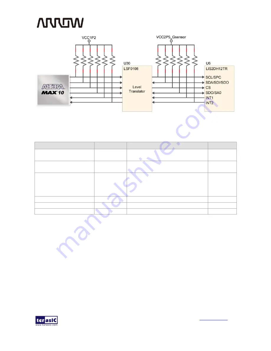
Figure 3-29 shows the connections between the MAX 10 FPGA and accelerometer sensor.
Table 3-20 Pin Assignment of Accelerometer Sensor
Signal Name
FPGA Pin No.
Description
I/O Standard
G_SENSOR_SDI
PIN_C6
I2C serial data/SPI serial data
input/3-wire interface serial dta output
1.2V
G_SENSOR_SDO
PIN_D5
SPI serial data output/I2C less
significant bit of the device address
1.2V
G_SENSOR_CS_n
PIN_E9
SPI enable, I2C/SPI mode selection: 1:
SPI idle mode/I2C communication
enabled, 0: SPI communication
mode/I2C disabled
1.2V
G_SENSOR_SCLK
PIN_B5
I2C serial clock/SPI serial port clock
1.2V
G_SENSOR_INT1
PIN_E8
Interrupt pin 1
1.2V
G_SENSOR_INT2
PIN_D7
Interrupt pin 2
1.2V
3.4.16
M
M
i
i
c
c
r
r
o
o
S
S
D
D
C
C
a
a
r
r
d
d
S
S
o
o
c
c
k
k
e
e
t
t
The board supports Micro SD card interface with x4 data lines. Through the load switches
(U25/U26) and voltage-translation transceiver (U22), user can select 1.8V or 3.3V VCCIO power of
Micro SD card to implement external storage application.
Figure 3-30
shows signals connected
between the MAX 10 FPGA and Micro SD card socket.
Table 3-21
lists the pin assignment of Micro SD card socket to the MAX 10 FPGA.


