background image

ADP1055-EVALZ User Guide 

UG-710


Rev. B | Page 7 of 43 

A pop-up window shows a notification of successful 
installation. 

12

386

-00

9


Figure 9. Successful GUI Installation 

Launching the GUI 

1.


Ensure that the evaluation board, the auxiliary power 
board, and the daughter card are already plugged into  
the main power board. If they are mishandled during 
shipment, ensure that they are properly attached as per 
Figure 1. 

2.


Ensure that the CTRL switch or hardware PSON (SW2) is 
turned to the Off position (switch position on the right). 

3.


Plug one end of the USB to I

2

C adapter in Jumper J6 or in 

the connector on the daughter card, and plug the other end 
in the USB port of the PC. 

4.


Launch the 

ADP1055

 GUI. The software GUI should 

report that the 

ADP1055

 has been located with the 

address. Click 

Finish 

to proceed. 

123

86-

0

10


Figure 10. Address Detection of 

ADP1055


5.


The 

ADP1055

 in the evaluation kit is preprogrammed with 

the board and command settings, so this step is optional. 
If you want to load the default command and board 
settings file from a local folder, click the 

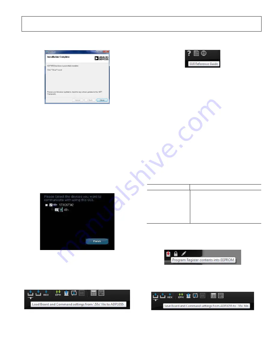
Load Command 

and Board settings from a ‘.55s’ file to ADP1055

 icon. 

12

38

6-

0

1

1


Figure 11. Leftmost Icon Shows Loading of .55s Settings File 

6.


Select the 

ADP1055240W.55s

 file. For more information 

about the 

ADP1055

 GUI, refer to the 

ADP1055

 GUI user 

guide by clicking on the leftmost question mark icon in the 
top section of the GUI. 

1

238

6-

01

2


Figure 12. Leftmost Icon Shows GUI Reference Guide 

POWERING UP 

1.


Connect a dc source (voltage range of 38 V dc to 60 V dc) 
at the input terminals and an electronic load at the output 
terminals. Refer to Figure 6 for the correct configuration. 

2.


Connect voltmeters on the input terminals and output 
terminals separately as shown in Figure 6. 

3.


Connect the voltage probes at different test pins. Ensure 
that the differential probes are used and that the ground of 
the probes are isolated if the measurements are made on 
the primary and secondary side of the transformer 
simultaneously. 

4.


Set the electronic load to 5 A. 

5.


Turn the CTRL switch (SW2) to the On position. 

The evaluation board should now be up and running, and ready 
for evaluation. The output should now read 12 V dc. 

After successful startup when the PSU is in steady state 
condition, LEDs provide the status of the board. 

Table 4. LED Indicators on the Evaluation Board 

LED Function 

D1 Input 

voltage 

D6 (Auxiliary Board) 

Auxiliary 9 V voltage on primary side 

D7 

Auxiliary 9 V voltage on secondary side 

D9 3.3 

that 

powers 

ADP1055

 IC 

D7 (Daughter Board) 

GPIO1 

D9 (Daughter Board) 

GPIO2 

After completing the programming of the 

ADP1055

, click the 

Program command and board contents into EEPROM

 icon to 

program the command and board settings into EEPROM to 
save the settings in the part. 

12

386

-013


Figure 

13

. Leftmost Icon Shows Store to EEPROM Option 

Use the 

Save Command and Board settings from ADP1055 to 

a ‘.55s’ fil

e icon to generate a .55s file to save the commands and 

board settings. 

1

2386-

014


Figure 

14

. Second Icon from the Left Shows Save to File Option 

Содержание ADP1055-EVALZ

Страница 1: ...ionality Droop current sharing On board tests for housekeeping functions PMBus communication Software GUI EVALUATION KIT CONTENTS ADP1055 EVALZ evaluation board ADP1055DC1 EVALZ daughter card ADDITION...

Страница 2: ...16 VOUT Window 16 IOUT Window 17 POUT Window 18 Temperature Window 18 PGOOD and GPIO Windows 19 32 Bit Keycode 19 Command Masking 19 Active Clamp Snubber 20 Digital Control Loop 22 Efficiency Curves 2...

Страница 3: ...ibed as follows The input filter consists of a single state LC L10 and C6 13 Components U2 and U5 are half bridge 4 A drivers based on the Analog Devices Inc iCoupler technology that provides gate dri...

Страница 4: ...ADP1055 daughter card connector J6 J7 I2 C connector J4 Auxiliary power board connector I2 C PMBus Connector on ADP1055 Daughter Card Table 2 J6 Connections Left to Right Pin Function 1 5 V 2 SCL 3 S...

Страница 5: ...dows XP 32 bit or Vista 32 bit Windows 7 32 64 bit and Windows 8 32 bit Precision digital multimeters HP34401 or equivalent USB to I2 C connector ADP I2C USB Z as shown in Figure 5 This must be ordere...

Страница 6: ...stallation file to start the installation Click Next 12386 007 Figure 7 GUI Installation 2 When the Total Phase USB Setup window appears click Next Read the license agreement check I accept the terms...

Страница 7: ...12 Leftmost Icon Shows GUI Reference Guide POWERING UP 1 Connect a dc source voltage range of 38 V dc to 60 V dc at the input terminals and an electronic load at the output terminals Refer to Figure 6...

Страница 8: ...ser Guide Rev B Page 8 of 43 12386 015 Figure 15 Main Setup Window of the ADP1055 GUI 12386 016 Figure 16 Monitor Window in the GUI For more information on the board settings refer to the GUI referenc...

Страница 9: ...ure 17 represent the signals at the output pins of the IC Although the switching frequency can be increased the software does not account for the dead times these have to be programmed manually by mea...

Страница 10: ...d What follows is an example that shows the effectiveness of the volt second balance feature A deliberate extra on time was added to one leg of the H bridge creating an imbalance in the transformer 12...

Страница 11: ...27 ADT Window Things to Try 1 Set up PWMs for additional topologies such as active clamp isolated boost and so on 2 Use the SYNC feature of the ADP1055 to synchronize to an external frequency CTRL AN...

Страница 12: ...WM To facilitate a proper soft start from the precharge prebias condition where the output bus has not yet discharged to zero the ADP1055 uses the SR phase in and SR transition function to ensure that...

Страница 13: ...at 20 A Load Yellow Trace Load Current Green Trace Output Voltage Red Trace SR1 When soft stop is initiated from light load mode SR1 and SR2 are initially off However to facilitate soft stop they tur...

Страница 14: ...fault ID FFID that caused the PSU to shutdown is displayed in a monitoring window A complete description of the fault response can be found in the data sheet 12386 038 Figure 38 VOUT_OV_FAST_FAULT Fa...

Страница 15: ...set up in the Fault Response window In the Additional Settings bar the voltage feedforward function can be enabled Since the ADP1055 is a secondary side controller the input voltage is not available t...

Страница 16: ...ching period depending upon the timeout value this is set in the Additional Settings bar For example a timeout of four switching cycles causes the IN_FAST_OC_FAULT flag to set when the IIN_FAST_OC_FAU...

Страница 17: ...12386 052 Figure 53 Output Voltage Ripple 20 A Load Green Trace AC Coupled Output Voltage IOUT WINDOW The IOUT window sets thresholds for the output current Thresholds for output over current under cu...

Страница 18: ...can be set Also the constant current averaging rate and the slew rate can be selected POUT WINDOW The threshold limit for over load power can be set in this window The settings can be changed in a si...

Страница 19: ...tions available for programming the output as shown in Figure 63 12386 062 Figure 63 Logic Options for GPIO 32 BIT KEYCODE The ADP1055 has a 32 bit password protection and extended command masking set...

Страница 20: ...a programmable on time and a delay from the reference PWM A complete description of the active snubber function is available in the data sheet 12386 068 Figure 69 Active Clamp Option in Evaluation Boa...

Страница 21: ...Source Voltage of Low Side SR FET Blue Trace Gate Source Voltage of Snubber FET Red Trace Drain Source Voltage of Snubber FET 12386 074 Figure 75 Active Clamp Snubber Enabled Zoomed In 10 A Load 50 n...

Страница 22: ...III compensator based on the stability rules Using the loop analyzer you can validate the programmed control loop as shown in Figure 78 For an easy test on the control loop the signal from loop analy...

Страница 23: ...gure 81 Transient Response with Load Steps 50 to 100 to 50 Green Trace AC Coupled Output Voltage Yellow Trace Load Current 1 A s 12386 081 Figure 82 Transient Response with Load Steps 25 to 50 to 25 G...

Страница 24: ...055 can be programmed to optimize performance when the output current drops below a certain level The light load and deep light load mode thresholds are set in a manner to reduce losses and increase e...

Страница 25: ...gure 88 Efficiency Curve at 36 V DC 48 V DC 60 V DC and 75 V DC Input 89 90 91 92 93 94 95 36 40 44 48 52 56 60 EFFICIENCY VIN V 20A LOAD 15A LOAD 10A LOAD 5A LOAD 12386 105 Figure 89 Efficiency vs In...

Страница 26: ...00h VIN_OFF Reg 37 h 0000h INTERLEAVE Reg 38 h B266h IOUT_CAL_GAIN Reg 39 h 8000h IOUT_CAL_OFFSET Reg 40 h 6C00h VOUT_OV_FAULT_LIMIT Reg 41 h FCh VOUT_OV_FAULT_RESPONSE Reg 42 h 6800h VOUT_OV_WARN_LIM...

Страница 27: ..._DIGFILT_HF_GAIN_SETTING Reg FE09 h 0Ch SS_DIGFILT_LF_GAIN_SETTING Reg FE0A h AEh SS_DIGFILT_ZERO_SETTING Reg FE0B h 00h SS_DIGFILT_POLE_SETTING Reg FE0C h 1Eh SS_DIGFILT_HF_GAIN_SETTING Reg FE0D h 33...

Страница 28: ...Reg FE38 h B8h ISHARE_FAULT_RESPONSE Reg FE39 h 3Fh GPIO1_FAULT_RESPONSE Reg FE3A h 38h GPIO2_FAULT_RESPONSE Reg FE3B h 3Fh GPIO3_FAULT_RESPONSE Reg FE3C h 38h GPIO4_FAULT_RESPONSE Reg FE3D h C0h PWM_...

Страница 29: ...Reg FE61 h 00h LOW_TEMP_POLE Reg FE62 h 01h LOW_TEMP_SETTING Reg FE63 h 13h GPIO3_4_SNUBBER_ON_TIME Reg FE64 h 4Ah GPIO3_4_SNUBBER_DELAY Reg FE65 h 80h VOUT_DROOP_SETTING Reg FE66 h 00h NL_BURST_MODE...

Страница 30: ...0 KOhm R4 0 KOhm C5 0 F C6 0 F R6 25 KOhm R7 1 KOhm Topology 0 0 Full Bridge 1 Half Bridge 2 Two Switch Forward 3 Interleaved Two Switch Forward 4 Active Clamp Forward Restricted_1 0 Restricted_2 0 Re...

Страница 31: ...SABLE 5 NC1 6 NC2 7 VDD1 8 GNDB 9 VOB 10 VDDB 11 NC3 12 NC4 13 GNDA 14 VOA 15 VDDA 16 C138 0 1 F VG_QB R167 1 R182 10k C12 2 2 F R180 1 QD IRFR540ZPBF 2 1 3 Q41 DNI 3 2 1 L8 24 H PA1494 242NL 1 2 Q23...

Страница 32: ...4 DNI R590 C61 220pF R10 10k J6 5V 1 SCL 2 SDA 3 GND 4 D76 MMBD7000HS 7 F 1 3 2 C58 33pF J4 VIN_AUX1 1 PRI_GND1 2 VIN_AUX2 3 PRI_GND2 4 VIN_AUX3 5 PRI_GND3 6 VDD_PRI1 7 VDD_PRI2 8 NC1 9 NC2 10 SPARE 1...

Страница 33: ...ADP1055 EVALZ User Guide UG 710 ADP1055 EVALZ LAYOUT 12386 092 Figure 93 PCB Assembly Top 12386 093 Figure 94 PCB Layout Silkscreen Layer 12386 094 Figure 95 PCB Layout Top Layer Rev B Page 33 of 43...

Страница 34: ...UG 710 ADP1055 EVALZ User Guide 12386 095 Figure 96 PCB Layout Layer 2 12386 096 Figure 97 PCB Layout Layer 3 12386 097 Figure 98 PCB Layout Layer 4 Rev B Page 34 of 43...

Страница 35: ...ADP1055 EVALZ User Guide UG 710 12386 098 Figure 99 PCB Layout Bottom Layout 12386 099 Figure 100 PCB Assembly Bottom Rev B Page 35 of 43...

Страница 36: ...RE BUS FEEDBACK PIN I2C SERIAL DATA INPUT AND OUTPUT I2C SERIAL CLOCK INPUT TEMPERATURE SYNCHRONIZATION GENERAL PURPOSE INPUT OUTPUT SMB ALERT POWER SUPPLY ON INPUT GENERAL PURPOSE INPUT OUTPUT PWM OU...

Страница 37: ...igure 102 PCB Assembly Top 12386 102 Figure 103 PCB Layout Silkscreen Layer Top 12386 103 Figure 104 PCB Layout Top Layer 12386 104 Figure 105 PCB Layout Layer 2 12386 105 Figure 106 PCB Layout Layer...

Страница 38: ...UG 710 ADP1055 EVALZ User Guide 12386 107 Figure 108 PCB Layout Silkscreen Bottom 12386 108 Figure 109 PCB Assembly Bottom Rev B Page 38 of 43...

Страница 39: ...C45 1 F CAP CER 1 F 25 V 10 X7R SMD Murata C1608X7R1E105K 1 C48 47 F CAP CER 47 F 16 V 10 X5R Murata GRM32ER61C476KE15K 1 C49 47 F CAP CER 47 F 16 V 10 X5R Murata GRM32ER61C476KE15K 1 C51 47 F CAP CE...

Страница 40: ...19 1 G_Q40 PC TEST POINT MINI SMD Keystone 5019 1 JP1 VIN CONN JACK BANANA UNINS PANEL MOU Emerson 108 0740 001 1 JP2 VIN CONN JACK BANANA UNINS PANEL MOU Emerson 108 0740 001 1 J1 BNC R CONN JACK VER...

Страница 41: ...RES 0 3 4 W 5 Vishay Dale 311 1 00CRCT ND 1 R60 SHORTPIN 1 R61 SHORTPIN 1 R62 0 RES 0 0 1 8 W JUMPER SMD Yageo RC0805JR 070RL 1 R63 205 RES 205 1 8 W 5 SMD Yageo RC0805JR 07100RL 1 R64 SHORTPIN 1 R65...

Страница 42: ...JR 070RL 1 SWA PC TEST POINT MINI SMD Keystone 5019 1 SW2 PSON SW SLIDE SPDT 30 V 0 2 A PC MOUNT E Switch EG1218 1 TP5 TEST POINT HAND MADE CRAFTS Analog Devices 1 TP6 TEST POINT HAND MADE CRAFTS Anal...

Страница 43: ...ct to the following additional limitations Customer shall not i rent lease display sell transfer assign sublicense or distribute the Evaluation Board and ii permit any Third Party to access the Evalua...

Отзывы: