ADM1060
Rev. B | Page 36 of 52
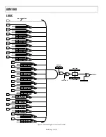
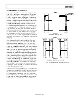
The functionality of the fault plane is best illustrated with an
example. For instance, take VP1 to have an input supply of 5.0 V.
A UV/OV window of 4.5 V to 5.5 V is set up on VP1. The
supply is ramped in and out of this window, each time reading
the contents of LATF1 and LATF2. The values recorded are as
follows:
1. VP1 at 5 V: LATF1 = LATF2 = 00000000. This is expected.
The supply is in tolerance, SFD output is 0, therefore no fault.
2. VP1 at 4.2 V: LATF1 = 10001000, LATF2 = 00000000. SFD
output has changed status to 1, therefore ANYFLT goes high.
3. VP1 at 5.0 V: LATF1 = 10000000, LATF2 = 00000000. SFD
output has changed status to 0, therefore ANYFLT goes high
again.
4. VP1 at 5.8 V: LATF1 = 10001000, LATF2 = 00000000. SFD
output again changed status from 0 to 1, so ANYFLT goes
high.
5. VP1 at 4.2 V: LATF1 = 10000000, LATF2 = 00000000. At first
glance, this would appear to be incorrect since the SFD out-
put should be at 1 (4.2 V is an undervoltage fault). However,
in ramping down from 5.8 V to 4.2 V, the supply passed into
the UV/OV window, the SFD output changed status from 1 to
0, ANYFLT was set high, and the register contents were
latched. It is these values that were read, before being reset by
reading LATF2.
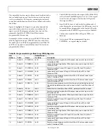
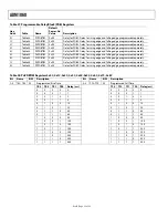
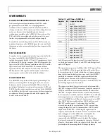
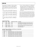
There are also two mask registers provided that enable the user
to ignore a fault on a given function. The bits of the error mask
registers are mapped in the same way as those of the fault regis-
ters with the exception that the ANYFLT bit cannot be masked.
Setting a 1 in the error mask register results in the equivalent bit
in the fault register always remaining at 0, regardless of whether
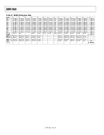
there is a fault on that function or not. The register and bit maps
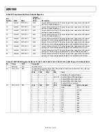
for both the fault and error mask registers are shown below.
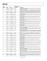
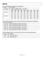
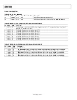
Table 42. Status Registers
Hex Addr.
Table
Name
Default Power-On Value
Description
D8
UVSTAT
0x00
Logic output of the UV comparator on each of the seven SFDs
D9
OVSTAT
0x00
Logic output of the OV comparator on each of the seven SFDs
DA
Table 45
SFDSTAT
0x00
Logic output (post Fault Type block) on each of the seven SFDs
DB
GWSTAT
0x00
Logic state of the four GPIs and the Watchdog Fault Detector
PDOSTAT1
0x00
Logic output of PDOs 1 to 8
DF
PDOSTAT2
0x00
Logic output of PDO 9
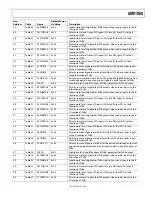
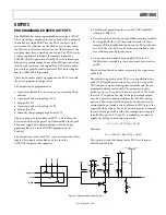
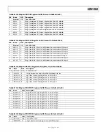
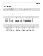
Table 43. Bit Map for UVSTAT Register 0xD8 (Power-On Default 0x00)
Bit Name
R/W Description
7
Reserved
N/A
Cannot Be Used
6
VP4UV
R
If high, voltage on VP4 input is lower than the UV threshold.
5
VP3UV
R
If high, voltage on VP3 input is lower than the UV threshold.
4
VP2UV
R
If high, voltage on VP2 input is lower than the UV threshold.
3
VP1UV
R
If high, voltage on VP1 input is lower than the UV threshold.
2
VHUV
R
If high, voltage on VH input is lower than the UV threshold.
1
VB2UV
R
If high, voltage on VB2 input is lower than the UV threshold.
0
VB1UV
R
If high, voltage on VB1 input is lower than the UV threshold.
Содержание ADM1060
Страница 51: ...ADM1060 Rev B Page 51 of 52 NOTES ...

