


ZYNQ Ultr FPGA Board AXU7EV User Manual
60 / 68
Amazon Store: https://www.amazon.com/alinx
Part 3.14: CAN Communication Interface
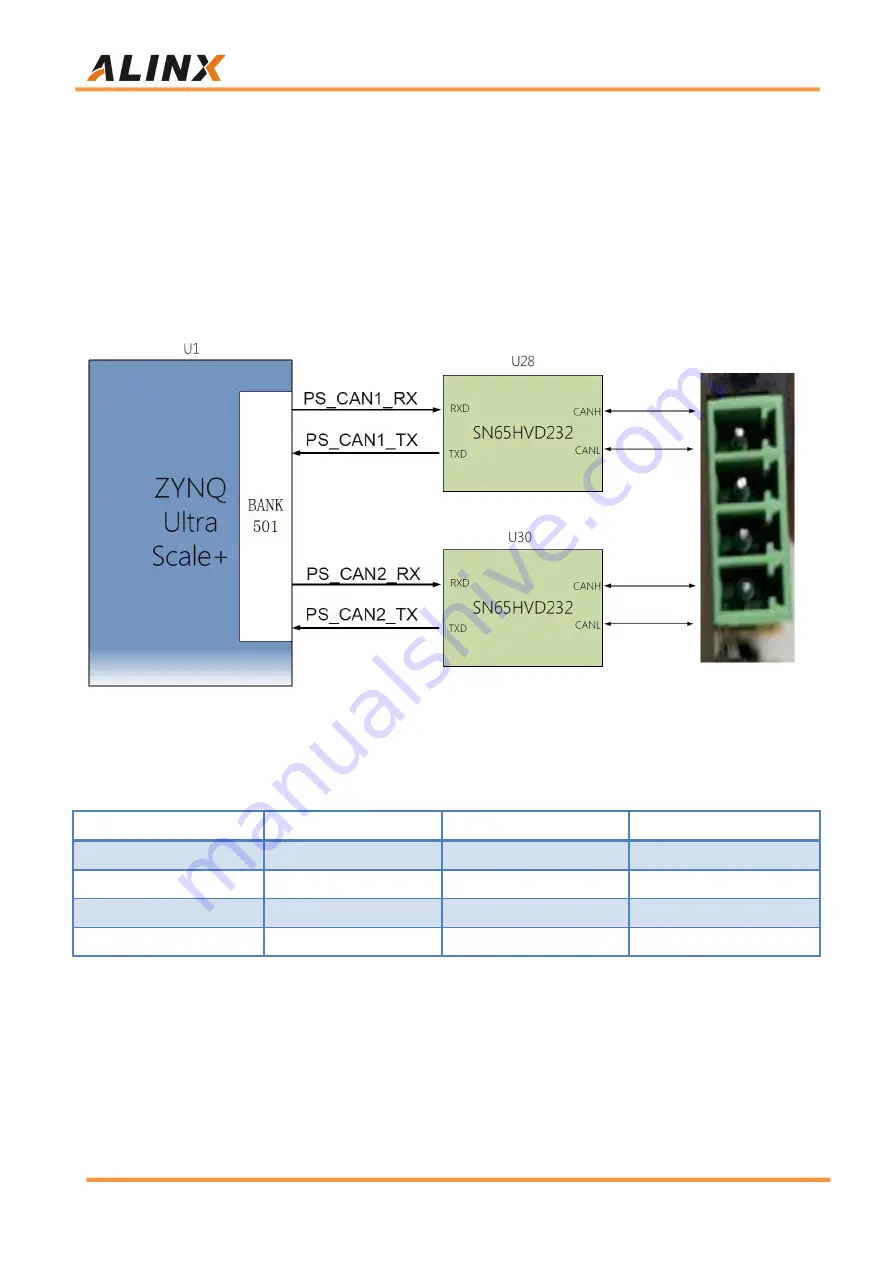
There are 2 CAN communication interfaces on the AXU7EV carrier board,
which are connected to the MIO interface of the BANK501 on the PS system
side. The CAN transceiver chip selected TI's SN65HVD232C chip for user CAN
communication services. The connection of the CAN transceiver chip on the
PS side is show as Figure 3-14-1
Figure 3-14-1: Connection diagram of CAN transceiver chip on PS side
The CAN communication pin assignments are as follows:
Signal Name
ZYNQ Pin Name
ZYNQ Pin Number
Description
PS_CAN1_RX
PS_MIO38
C34
CAN1 Receiver
PS_CAN1_TX
PS_MIO39
D30
CAN1 Transmitter
PS_CAN2_RX
PS_MIO41
D32
CAN2 Receiver
PS_CAN2_TX
PS_MIO40
D31
CAN2 Transmitter
Part 3.15: 485 Communication Interface
There are two 485 communication interfaces on the AXU7EV carrier board.
The 485 communication port is connected to the IO interface of BANK88 on the
PL system. The 485 transceiver chip selects the MAX3485 chip from MAXIM