– 38 –
RF I
RF O
RF M
RFTC
LD
PD
PD1, PD2
FE
F, E
EI
VEE
TEO
LPFI
TEI
ATSC
TZC
TDFCT
VC
FZC
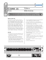
Pin No.
Pin Name
I/O
Description
32
33
34
35
36
37
38, 39
40
41, 42
43
44
45
46
47
48
49
50
51
52
I
O
I
I
O
I
I
I/O
I
—
—
O
I
I
I
I
I
O
I
Input terminal by capacity combination of RF summing amplifier.
Output terminal of RF summing amplifier. Checkpoint of Eye pattern.
Anti-reverse input terminal for RF summing amplifier.
The gain of RF amplifier is decided by the connection resistance between RF M and
RF O terminals.
This is a pin where the selection time constant is externally connected to control the
RF level.
APC amplifier output terminal.
APC amplifier input terminal.
RFI-V amplifier inverted input pin.
These pins are connected to the A+C and B+C pins of the optical pickup, receiving by
currents input.
Bias adjustment pin of the focus error amplifier. (Not used)
F and EIV amplifier inverted input pins.
These pins are connected to the F and E of the optical pickup, receiving by current
input.
Gain adjustment pin of the I-V amplifier E. (When not in use of BAL automatic
adjustment). (Not used)
GND connection pin.
Output terminal for tacking-error amplifier. Output E-F signal.
BAL adjustment comparator input pin. (Input through LPF from TEO)
Input terminal for tracking error.
Window-comparator input terminal for detecting ATSC.
Input terminal for tracking-zero cross comparator.
Capacitor connection pin for the time constant used when there is defect.
Output terminal for DC voltage reduced to half of VCC+VEE.
Input terminal for focus-zero cross comparator.
Содержание FM-LMD811
Страница 15: ...SCHEMATIC DIAGRAM 1 POWER PWR AMP PT MAIN PT SUB TU INF JACK 15 ...
Страница 17: ... 17 SCHEMATIC DIAGRAM 2 FRONT LED 1 LED 2 LED 3 ...
Страница 18: ...WIRING 6 TUNER 15 14 13 12 11 10 9 8 7 6 5 4 3 2 1 A B C D E F G H I J K L M N O P Q R S T U 18 ...
Страница 19: ...SCHEMATIC DIAGRAM 3 TUNER 19 ...
Страница 20: ...IC BLOCK DIAGRAM 20 ...
Страница 21: ... 21 LCD DIAGRAM LCD ASSY ACJ 6 ...
Страница 31: ...SCHEMATIC DIAGRAM 1 FUNC FRONT POWER KEY MOTOR DOOR SW LED L LED R 31 ...
Страница 34: ... 34 SCHEMATIC DIAGRAM 2 CD 1 2 ...
Страница 35: ...SCHEMATIC DIAGRAM 3 CD 2 2 35 ...
Страница 36: ...IC BLOCK DIAGRAM 36 ...
Страница 60: ... 60 CD MECHANISM EXPLODED VIEW 1 1 2 4 5 9 3 1 8 7 10 D D A C B 6 ...
Страница 64: ...2 11 IKENOHATA 1 CHOME TAITO KU TOKYO 110 JAPAN TEL 03 3827 3111 Printed in Singapore 9820572 0251431 ...