IntelliPack Series 892M/894M Computation Transmitter User's Manual DC Voltage/Current Input
___________________________________________________________________________________________
- 9 -
General Input Specifications
Input Accuracy:
Better than
0.05% of input span, typical.
Better than
0.3% of input span, typical for 0-1mA range.
This includes the effects of repeatability, but not sensor
error. This refers to input accuracy only, but does not
include analog output accuracy (see Table 6). Add input
accuracy to output accuracy to obtain worst case
inaccuracy from input to output for a given I/O
configuration.
Accuracy Versus Temperature:
Better than ±0.005% of
input span per
C, or
1uV/
C, whichever is greater.
Resolution:
See Table 5.
Input Bias Current:
±100nA maximum, excluding excitation
current of process current inputs.
Input Filter:
Normal mode filtering, plus digital filtering,
optimized and fixed per input range within the
-
ADC.
Noise Rejection (Normal Mode):
40dB @ 60Hz, typical
with 100
input unbalance (49.9
for process currents).
Noise Rejection (Common Mode):
100dB @ 60Hz, typical
with 100
input unbalance (49.9
for process currents).
Analog to Digital Converter (A/D):
A
16-bit
-
converter,
Analog Devices AD7714AR-5.
Input Conversion Rate:
5 conversions per second per
channel (894M), 8 conversions per second per channel
(892M).
Input Excitation Supply:
+15V DC typical with respect to
input common (COM), current limited to approximately
50mA. For use with two-wire process current
transmitters. This will power up to two 2-wire
transmitters.
Input Scaling:
The configuration software is used to scale
the nominal input signal range endpoints indicated, to
values representative of the your application’s
engineering units. Constants are limited to 8 characters
and may be entered as floating point numbers or using
scientific notation. If you wish to use a subset of the
nominal input range, then you will have to extrapolate the
corresponding scaling values as required.
HOLD (External Input Terminal):
A TTL or open
collector/drain signal (5V logic) may be wired directly to
the HOLD and COM terminal of the module to hold the
transmitter’s output at the last value while HOLD is
asserted. HOLD is asserted low and pulled-up internally.
The HOLD circuit is part of the input circuitry and is
isolated from the output circuit.
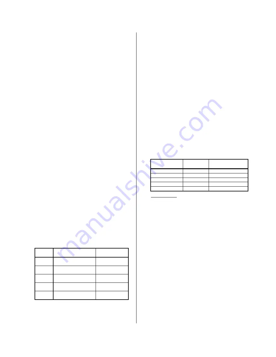
Table 5: Effective Resolution Per Nominal Input Range
Gain A
V
Nominal Input Range
Effective Bits/
A/D Resolution
128
0-1mA DC
16797/
60nA/LSB
8
0-20mA DC
20996/
953nA/LSB
8
4-20mA DC
16797/
953nA/LSB
2
0-5V DC
26298/
190uV/LSB
1
0-10V DC
26298/
380uV/LSB
IMPORTANT:
Input COM and RTN are not the same
potential and should never be connected together, either
directly or through ground. Do not tie COM to ground.
ANALOG OUTPUT SPECIFICATIONS
These units contain an optically isolated DAC (Digital-to-Analog
Converter) that provides a process current or voltage output.
Note that calibration can only occur with respect to one of the
outputs, voltage or current, and only one of the outputs may
operate at a t
ime. A jumper is required between the output “I+”
and “JMP” terminals for voltage output. Remove this jumper for
current output.
Voltage Output Specifications:
Output Range:
0-10V DC, 0-5V DC.
Output Accuracy:
See Table 6.
Output Current:
0-10mA DC maximum.
Output Impedance:
1
.
Output Resolution:
See Table 6.
Output Short Circuit Protection:
Included
Current Output Specifications:
Output Ranges:
0-20mA DC, 4-20mA DC, or 0-1mA DC.
Output Maximum Current:
21.6mA typical.
Output Accuracy:
See Table 6.
Output Compliance:
10V Minimum, 12V Typical.
Output Resolution:
See Table 6.
Output Load Resistance Range:
0 to 550
, typical.
Table 6: Analog Output Range Resolution & Accuracy
Output Range
Resolution
Output Accuracy
1,2
Percent-of-Span
0 to 20mA DC
0.0025%
0.025%
4 to 20mA DC
0.0025%
0.025%
0 to 1mA DC
0.0370%
0.300%
0 to 10V DC
0.0025%
0.025%
0 to 5V DC
0.0030%
0.050%
Notes (Table 6):
1. Voltage outputs unloaded. Loading will add “I*R” error.
2. Software calibration produces high overall accuracy.
3. All output current and voltage ranges are subsets of the
0-20mA range.
4. Worst case input-to-output inaccuracy can be calculated
by adding input accuracy to output accuracy.
General Output Specifications
Digital-to-Analog Converter:
Analog Devices AD420AR-32,
16-bit
-
. Monotonic to 16 bits.
Integral Non-Linearity:
0.002% (
1.4LSB) of span typical,
0.012% (
7.9LSB) of span maximum, for ranges utilizing
full output span (0-24mA, 0-10V DC).
Output Temperature Drift:
Better than
20ppm/
C Typical,
50ppm/
C Maximum.
Output Response Time:
800ms, typical, to 98% of output
transition with a step change in the input.
Output HOLD Function:
A TTL or open collector/drain
signal (5V logic) may be wired directly to the HOLD and
COM terminals of the module to hold the transmitter’s
output at the last value. HOLD is asserted low and
pulled-up internally. The HOLD circuit is part of the input
circuit and isolated from the output circuit. Note that
input COM and RTN terminals are not equivalent
potentials and should never be tied together, either
directly or through ground. Be careful when making earth
ground connections that input COM is not tied to earth
ground, which may be connected to input RTN.

