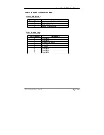
Appendix B Technical Summary
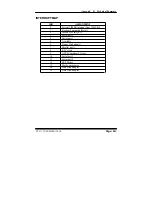
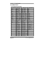
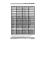
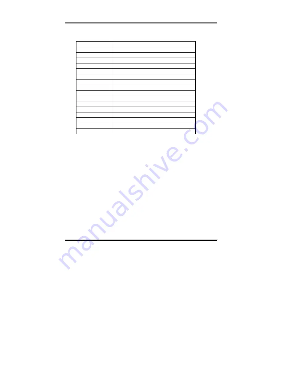
INTERRUPT MAP
IRQ ASSIGNMENT
0
System TIMER interrupt from TIMER-0
1
Keyboard output buffer full
2
Cascade for IRQ 8-15
3 Serial
port
2
4 Serial
port
1
5 Available
6 Floppy
Disk
adapter
7 Parallel
port
1
8 RTC clock
9 ACPI-Compliant System
10 Serial
port
3
11 Serial
port
4
12 PS/2 Mouse
13 Math coprocessor
14 Hard
Disk
adapter
15 Hard
Disk
adapter
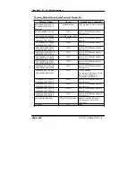
PC 5171 USER
c
S MANUAL
Page: B-3
Содержание PC 5171
Страница 1: ...USER S MANUAL PC 5171 Socket 478 P4 P4 M 17 inch Panel PC System...
Страница 9: ...Chapter 1 Introduction 1 2 CASE ILLUSTRATION PC 5171 USERc MANUAL Page 1 3...
Страница 21: ...Chapter 2 Hardware Configuration JUMPER DIAGRAMS JUMPER SETTINGS PC 5171 USER S MANUAL Page 2 5...
Страница 25: ...Chapter 2 Hardware Configuration RI 15 16 COM2 Max 1A 5V 4 6 12V 2 4 PC 5171 USER S MANUAL Page 2 9...
Страница 26: ...Chapter 2 Hardware Configuration RI 17 18 COM3 Max 1A 5V 7 9 12V 9 11 Page 2 10 PC 5171 USER S MANUAL...
Страница 27: ...Chapter 2 Hardware Configuration RI 19 20 COM4 Max 1A 5V 8 10 12V 10 12 PC 5171 USER S MANUAL Page 2 11...
Страница 92: ...Appendix A System Assembly EXPLODED DIAGRAM FOR REMOVING HOOK HOLDER PC 5171 USERcS MANUAL Page A 3...
Страница 93: ...Appendix A System Assembly EXPLODED DIAGRAM FOR REMOVING EXT CASE Page A 4 PC 5171 USERcS MANUAL...
Страница 94: ...Appendix A System Assembly EXPLODED DIAGRAM FOR REMOVING BACK COVER PC 5171 USERcS MANUAL Page A 5...
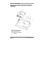
Страница 95: ...Appendix A System Assembly EXPLODED DIAGRAM FOR REMOVING LCD ASSEMBLY Diagram 1 Page A 6 PC 5171 USERcS MANUAL...
Страница 96: ...Appendix A System Assembly Diagram 2 PC 5171 USERcS MANUAL Page A 7...
Страница 97: ...Appendix A System Assembly EXPLODED DIAGRAM FOR FRONT PANEL Diagram 1 Page A 8 PC 5171 USERcS MANUAL...
Страница 98: ...Appendix A System Assembly Diagram 2 PC 5171 USERcS MANUAL Page A 9...
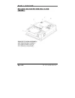
Страница 99: ...Appendix A System Assembly EXPLODED DIAGRAM FOR REMOVING CD ROM ASSEMBLY Page A 10 PC 5171 USERcS MANUAL...
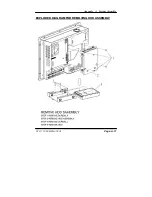
Страница 100: ...Appendix A System Assembly EXPLODED DIAGRAM FOR REMOVING HDD ASSEMBLY PC 5171 USERcS MANUAL Page A 11...
Страница 101: ...Appendix A System Assembly EXPLODED DIAGRAM FOR REMOVING MOTHERBOARD AND POWER Page A 12 PC 5171 USERcS MANUAL...
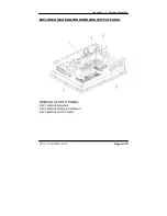
Страница 102: ...Appendix A System Assembly EXPLODED DIAGRAM FOR REMOVING OUTPUT PANEL PC 5171 USERcS MANUAL Page A 13...
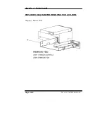
Страница 103: ...Appendix A System Assembly EXPLODED DIAGRAM FOR REMOVING FDD CD ROM Diagram 1 Remove FDD Page A 14 PC 5171 USERcS MANUAL...
Страница 104: ...Appendix A System Assembly Diagram 2 Remove CD ROM PC 5171 USERcS MANUAL Page A 15...
Страница 105: ...Appendix A System Assembly EXPLODED DIAGRAM FOR REMOVING MASK Page A 16 PC 5171 USERcS MANUAL...
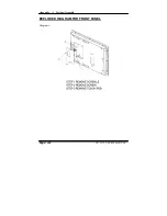
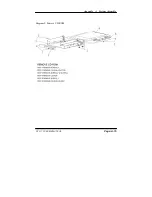
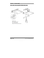
Страница 106: ...Appendix A System Assembly EXPLODED DIAGRAM FOR WALL MOUNTING Diagram 1 PC 5171 USERcS MANUAL Page A 17...
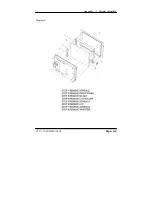
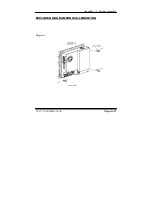
Страница 107: ...Appendix A System Assembly Diagram 2 Page A 18 PC 5171 USERcS MANUAL...
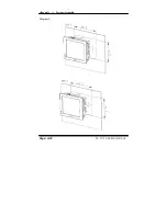
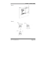
Страница 108: ...Appendix A System Assembly Diagram 3 Diagram 4 PC 5171 USERcS MANUAL Page A 19...
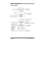
Страница 110: ...Appendix B Technical Summary BLOCK DIAGRAM Page B 2 PC 5171 USERcS MANUAL...


