A
B
C
D
E
F
G
H
1
2
3
4
5
6
I
J
K
L
7
8
GX-900
■
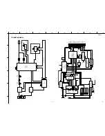
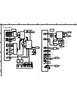
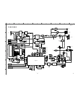
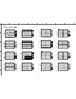
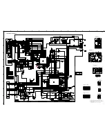
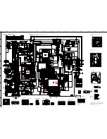
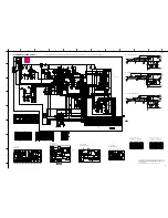
SCHEMATIC DIAGRAM (MD)
* All voltage are measured with a 10M
Ω
/V DC electric volt meter.
* Components having special characteristics are marked
Z
and
must be replaced with parts having specifications equal to those
originally installed.
* Schematic diagram is subject to change without notice.
85
IC4 : TC74HCT04AF-T1
Hex Inverters
IC3, 5 :
µ
PC4570G2
Dual OP-Amp
–
+
OUT
1
–IN
1
–V
CC
+V
CC
OUT
2
1
2
3
4
5
+IN
1
–IN
2
+IN
2
–
+
6
7
8
1A
1Y
2Y
V
DD
6A
1
2
3
4
11
2A
6Y
5A
12
13
14
3A
3Y
5Y
4A
5
6
7
V
SS
4Y
8
9
10
Point
i
(Pin13 of IC2)
V : 2V/div
H : 50 nsec/div
DC range
1 : 1 probe
0V
LPF
MUTING
MD CPU
REGULATOR
BACKUP
BUFFER
0
0
4.8
-9.8
0
0
0
0
0
0
0
0
0
0
0
0
0
0
0
0
0
0
0
0
0
0
0
0
0
0
0
0
0
0
0
0
0
0
0
0
0
0
0
0
0
0
0
0
0
0
0
0
0
0
0
4.6
0
0
0
4.6
0
0
0
0
4.2
0.1
4.6
4.5
0
2.2
0
0
0
4.7
0
0
0
0
0
0
0
0
0
0
0
0
4.7
4.7
2.3
0
2.1
4.7
4.7
4.7
5.1
5.1
5.5
5.5
4.7
10.9
10.3
0
0
0
1.2
1.2
5.0
10.1
0
0
0
-9.8
0
0
0
-9.8
-9.8
0
0
0
5.0
5.5
5.0
3.1
3.4
5.5
3.8
3.8
0
5.0
0
2.0
0
0
0
0
-9.8
0
0
12.4
6.0
6.6
6.6
0
10.1
0
~
~
~
~
~
~
~
i
5
6
8
7
2
3
4
4
1
2
3
1
5
6
8
7
P84
K-7
P87
C-9
P87
E-8
P89
A-3
P87
B-9
Summary of Contents for GX-900
Page 103: ...GX 900 GX 900 ...

