background image

GX-900

GX-900

1 0 0 6 7 4

SERVICE MANUAL

GX-900

MINI COMPONENT SYSTEM

IMPORTANT NOTICE

This manual has been provided for the use of authorized YAMAHA Retailers and their service personnel.
It has been assumed that basic service procedures inherent to the industry, and more specifically YAMAHA Products, are
already known and understood by the users, and have therefore not been restated.

WARNING:

Failure to follow appropriate service and safety procedures when servicing this product  may result in
personal injury, destruction of expensive components, and failure of the  product to perform as specified.
For these reasons, we advise all YAMAHA product owners that any service required should be performed
by an authorized YAMAHA Retailer or the appointed service representative.

IMPORTANT:

The presentation or sale of this manual to any individual or firm does not constitute authorization,  certifica-
tion  or  recognition  of  any  applicable  technical  capabilities,  or establish a principle-agent relationship
of any form.

The data provided is believed to be accurate and applicable to the unit(s) indicated on the cover.  The research, engineering, and
service departments of YAMAHA are continually striving  to improve YAMAHA products. Modifications are, therefore,
inevitable and specifications are subject to change without notice or obligation to retrofit. Should any discrepancy appear to
exist, please contact the distributor's Service Division.

WARNING:

Static discharges can destroy expensive components. Discharge any static electricity your body may have
accumulated by grounding yourself to the ground buss in the unit (heavy gauge black wires connect to this
buss).

IMPORTANT:

Turn the unit OFF during disassembly and part replacement. Recheck all work before you apply power to the
unit.

CONTENTS

TO SERVICE PERSONNEL ..................................... 1~2
FRONT PANELS ........................................................... 3
REAR PANELS ............................................................. 4
SPECIFICATIONS ......................................................... 5
INTERNAL VIEW .......................................................... 6
DISASSEMBLY PROCEDURES ............................ 7~16
VOLUME RANGE ....................................................... 17
SYSTEM CONTROL CHECK ..................................... 17
TEST MODE ................................................................ 18
SYSTEM TEST MODE ................................................ 18
RECEIVER TEST MODE ...................................... 19~20
TAPE TEST MODE ..................................................... 20
CD TEST MODE ......................................................... 21
ALL FUNCTION TEST MODE .................................... 22
CD ERROR MESSAGES ............................................ 22
CD STANDARD OPERATION CHART ................ 23~26

TAPE ADJUSTMENTS ......................................... 27~29
MD TEST MODE & ADJUSTMENTS ................... 30~37
MD ERROR DISPLAY .......................................... 38~39
MD TROUBLESHOOTING .................................... 40~44
IC DATA ................................................................ 45~58
DISPLAY DATA .......................................................... 59
BLOCK DIAGRAM ................................................ 60~65
MD TEST POINT WAVEFORM ............................ 66~67
PRINTED CIRCUIT BOARD ................................. 68~82
PIN CONNECTION DIAGRAM ................................... 83
SCHEMATIC DIAGRAM ....................................... 84~90
PARTS LIST ........................................................ 91~117
GREASE APPLICATION DIAGRAM ................ 118~120
REMOTE CONTROL TRANSMITTER ...................... 121
NX-GX500 .................................................................. 122

このサービスマニュアルは、エコマーク認定の再生紙を使用しています。
This Service Manual uses recycled paper.

GX-900 is composed of GX-900 and NX-GX500.

Summary of Contents for GX-900

Page 1: ...g to improve YAMAHA products Modifications are therefore inevitable and specifications are subject to change without notice or obligation to retrofit Should any discrepancy appear to exist please contact the distributor s Service Division WARNING Static discharges can destroy expensive components Discharge any static electricity your body may have accumulated by grounding yourself to the ground bu...

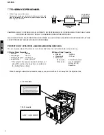
Page 2: ...OTHER THAN THOSE SPECIFIED HEREIN MAY RESULT IN HAZARDOUS RADIATION EXPOSURE THE COMPACT DISC PLAYER MINI DISC RECORDER SHOULD NOT BE ADJUSTED OR REPAIRED BY ANYONE EXCEPT PROPERLY QUALIFIED SERVICE PERSONNEL 1 q B G models w B G models AC LEAKAGE TESTER OR EQUIVALENT EQUIPMENT UNDER TEST INSULATING TABLE WALL OUTLET MD Laser Diode Properties Material GaAlAs Wavelength 785 nm Pulse time Read mode ...

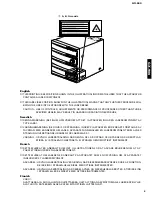
Page 3: ...NT SOM AVGER STRÅLNING ÖVERSTIGANDE GRÄNSEN FÖR LASERKLASS 1 VARNING OSYNLIG LASERSTRÅLNING NÄR DENNA DEL ÄR ÖPPNAD OCH SPÄRREN ÄR URKOPPLAD STIRRA EJ I STRÅLEN OCH BETRAKTA EJ STRÅLEN GENOM OPTISKT INSTRUMENT Danish DETTE MÆRKAT ER ANBRAGT SOM VIST I ILLUSTRATIONEN FOR AT ADVARE BRUGEREN OM AT AP PARATET INDEHOLDER EN LASERKOMPONENT DETTE MÆRKAT OM LASEREN ER ANBRAGT PÅ APPARATET SOM EN OPLYSNING...

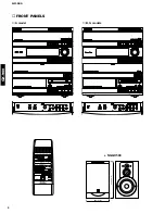
Page 4: ...W X Y Z 2 2 3 3 4 4 5 5 6 6 7 7 8 8 R TIME C EDIT D I0 E MODE REPEAT RANDOM SPACE TUNER DISC SKIP POWER SLEEP INPUT VOLUME 9 0 PRESET TIME A PROG B CD I YMERSION BASS BOOST MUSIC INPUT MODE M MARK SCROLL TAPE MD REC PAUSE ENTER DELETE REC PAUSE DIRECTION MD EDIT SYS20 200 7 7 8 320 12 5 8 NX GX500 ...

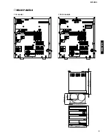
Page 5: ...GX 900 GX 900 A model B G models 4 343 13 1 2 12 1 2 9 3 8 364 14 5 16 100 3 15 16 172 6 3 4 280 11 320 12 5 8 REAR PANELS ...

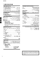
Page 6: ...3dB S N Ratio NR off 58dB Dolby B NR on 66dB MD SECTION System Minidisc digital audio system Recording Method Magnetic field moduration overwrite Reading Method Non contact optical pick up Coding ATRAC Adaptive TRansform Acoustic Coding Laser Diode Properties Meterial GaALAs Wavelength 785 nm Pulse time Read mode 0 8 mW continuous Write mode max 10 mW 0 5S min cycle 1 5S Repetition SPEAKER SECTION...

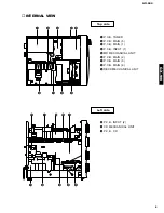
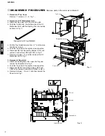
Page 7: ...op side q P C B TUNER w P C B MAIN 5 e P C B MAIN 1 r P C B INPUT 1 t MD MECHANICAL UNIT y P C B MAIN 2 u P C B MAIN 3 i P C B MAIN 6 o DECK MECHANICAL UNIT 0 P C B INPUT 2 1 CD MECHANICAL UNIT 2 P C B CD q w e r t i o y 0 q 1 2 r u u y i o t ...

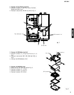
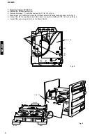
Page 8: ...tion e Disconnect the Flat Connecting Cables CB9 and remove 2 connectors CB8 and CB7 in Fig 2 f Remove 4 screws w and then remove the CD Mechanical Unit in Fig 1 Ejecting Tool for CD Tray TX946040 3 Removal of Panel Unit a Rotate the Loading Gear then open the Tray and remove the Cassette Lid in Fig 2 b Push the Tray back to the original closed position c Disconnect the flat connecting cables CB10...

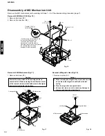
Page 9: ... Mechanical Unit a Remove 3 screws y in Fig 3 and 1 screw u in Fig 1 b Remove 4 connectors CB1 CB3 CB4 and CB5 in Fig 3 c Remove the MD Mechanical Unit y Bottom side y MD Mechanical Unit CB3 CB5 CB1 CB4 6 Removal of MD Mechanism a Disconnect the flat connecting cable in Fig 4 b Remove 4 screws i in Fig 4 c Remove 2 screws o in Fig 4 d Remove 2 screws 0 in Fig 4 P C B MD MD Mechanism Fig 4 i i o o ...

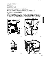
Page 10: ...n remove the P C B CD in Fig 5 c Place blocks at 3 locations to hold the CD Mechanical Unit horizontally as shown in the Fig 6 d Connect the Flat Connecting Cable CB9 and 2 connectors CB8 and CB7 in Fig 5 and Fig 6 e Connect the power plug and turn on the Power Switch 1 CB9 CB8 CB7 P C B CD Block Block P C B CD Block ...

Page 11: ... to the main unit in Fig 10 k Connect the flat connecting cables CB10 and CB13 and remove a connector CB805 in Fig 2 l Connect the power plug and turn on the Power Switch Fig 10 10 2 2 2 3 4 P C B Main 2 5 5 P C B Input P C B Main 1 CAUTION When the power to this equipment is turned on with the CD MD Mechanical Unit disconnected the capacitor C255 4700 16 of the Main P C B CD MD power supply secti...

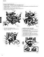
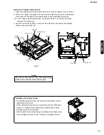
Page 12: ...t of the Friction Gear into the groove in the Tray Installation of Traverse Unit Slider a Fit the Traverse Unit into the Chassis b Turn the Cam Gear until its Guide Pin comes to the position as shown in Fig 12 c Fit the Slider into the Traverse Unit Set the Spring of the Slider so that it holds down the Guide Pin of the Cam Gear as shown in Fig B Press the Spring of the Slider once and release it ...

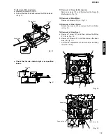
Page 13: ...then remove the Pinch Roller in Fig 15 14 Removal of Head Ass y a Remove 1 screw 1 and then remove the Relay P C B in Fig 15 b Remove 2 screws 2 and then remove the Head Ass y in Fig 15 Perform the adjustment of azimuth after installing the Head Ass y 10 Removal of Pick up Head a Remove the Gear A in Fig 13 b Pull out the Sled Shaft and remove the Pick up Head in Fig 13 Check that the disc table h...

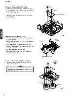
Page 14: ...of MD Main P C B Fig 16 1 Remove 4 screws Q1 2 Remove 6 connectors Q2 Removal of MD Mechanism Fig 17 1 Remove 4 screws R1 Caution Almost the entire surface of the cartridge holder is coated with oil When removing the mechanism hold it at the rear end where marked with arrows in the figure and avoid touching the oiled surface Fig 17 Fig 16 Flexible P C B for optical pickup 1 MD Main P C B 1 After p...

Page 15: ... it to the left Slider Lever Cartridge Holder Clamper Lever Rack Gear Roller Arm Lever Loading Motor Cam Plate Lever B1 x1 Ø1 7x5mm B2 x1 Fig 19 Caution Be careful so that oil does not get on the clamper lever which contacts the roller of the roller arm lever Installation of Cartridge Holder To install the cartridge holder the rack of the mechanism must be lowered toward the rear While pushing the...

Page 16: ...P C B Loading Motor Sled motor Caution Use care so as not to cause any damage to the gear The damaged gear will cause abnormal noise to occur while searching Installation of Mechanism SW P C B Set the mechanism to the eject mode by applying 5V to the loading motor Install the mechanism SW P C B so that the boss fits in the hole in it Push the lead switch on the mechanism SW P C B toward the optica...

Page 17: ...tor is removed it will be neces sary to perform Pickup Rating See page 35 1 Remove 3 screws C1 2 Remove the spindle motor by moving it in the arrow direction Caution a Be careful not to scratch the gear Scratched gear will produce noises during searching b As the turn table is magnetized keep foreign objects from being attracted C1 x1 Ø1 7x2 1mm C1 x3 Ø1 7x2 5mm F1 x3 Ø1 7x9 5mm Turn Table Spindle...

Page 18: ...ON CD DISC No display on no In case that CD doesn t play RECEIVER CD SYSCK CDCE SYSO NG In case that DISPLAY doesn t change CD RECEIVER SYSI NG yes q FUNCTION AUX is selected CD PLAY KEY ON remote control transmitter 17 SYSCK Pin 20 of IC8 CDCE Pin 25 of IC8 SYSO Pin 21 of IC8 SYSI Pin 22 of IC8 r FUNCTION MD MD display on no In case that MD doesn t play RECEIVER CD SYSCK CDCE SYSO NG In case that...

Page 19: ...ctors for power off at starting Display Description Key Operate Power off by button operation Off Timer Power off by Off Timer setting Sleep Timer Power off by Sleep Timer function Auto Off Power off by Auto Power Off function I Protect Power off by detection of an abnormal current value V Protect Power off by detection of an abnormal voltage value Temp Over Power off by detection of an abnormal t...

Page 20: ...ht up for 2 seconds and RAM of CPU is initialized The product mode is restored Presetting of the tuner becomes the manufacturer preset state Used to check lighting of all display segments At the first pressing of the STANDBY ON button all display segments light up and at the second pressing this mode is canceled The product mode is restored Do not use No 04 to 23 functions as they are not for serv...

Page 21: ...1 When the equalizer test mode is set GEQ xxx is displayed xxx represents the 3 band value of GEQ It is possible to set the GEQ value directly using the buttons on the remote control unit Example To obtain flat GEQ 6 6 6 Low tone Intermediate tone High tone Displayed value 0 1 2 3 4 5 6 7 8 9 A B C Gain dB 12 10 8 6 4 2 0 2 4 6 8 10 12 Operation Procedure To set a value for each band 0 to 9 A TIME...

Page 22: ...k Displayed servo coefficient address up 1 track kick Displayed servo coefficient address down Enter normal operation 1 track kick Displayed servo coefficient without mecha INIT increment Enter normal operation 30 track kick Displayed servo coefficient decrement Start TEST REPEAT 30 track kick Send the displayed servo Do not use this function as coefficient 2 it is not for servicing 1 Adj lights d...

Page 23: ...E E AF MN ERR CONTENTS OF ERROR CD fails in the disc data reading after the state shift CD fails in the disc data reading CD fails in the TOC data reading Tracking servo is not effective at the disc motor servo PLL Disc motor servo PLL is not effective CD fails in focus search CD fails in escaping from the lead in area The inner limit switch does not operate at the feed inner control CD fails in r...

Page 24: ... mechanism unit clamped up Feed inward switch research Laser ON Disc scan FOCUS Gain rough ADJ FOCUS Search operation FOCUS LOCK servo ON Spindle motor accelerated TRACKING servo ON Disc servo ON VCO lock Tracking Gain rough ADJ Tracking Balance ADJ only Tray OPEN CLOSE OPEN appears in the TIME indicator TRV signal is output until detection of LIMIT switch DISC 1 is turned to DM clamp position LDO...

Page 25: ...ching the beginning MUTE is cancelled PLAY MUTE ON Spindle motor stop Laser OFF Forced feed return STOP MUTE L H 0 00 appears in the time indicator IC11 64 pin TOC READ After searching the beginning MUTE is cancelled Press the STOP key MUTE H L MUTE L H 0 00 appears in the time indicator LDON H L IC5 40 pin FLSW L IC11 26 pin A ...

Page 26: ... OFF YES 10sec timer start LOAD MOTOR STOP END 10sec timer time up NO YES LOAD MOTOR STOP ERROR NO TIMER 10ms UNLOAD SW OFF YES NO DOWN operation LOAD MOTOR forward rotate Start DOWN SW ON YES 10sec timer start END 10sec timer time up NO YES LOAD MOTOR STOP ERROR NO TIMER 10ms DOWN SW ON YES NO LOAD MOTOR forward rotate Start LOAD SW ON YES 10sec timer start LOAD MOTOR STOP END 10sec timer time up...

Page 27: ... YES DISC NO count STOP SW OFF YES DISC NO 3 YES DISC NO clear NO ROTARY MOTOR retard STOP SW ON NO YES ROTARY MOTOR STOP ROTARY MOTOR 32ms back pluse STOP SW ON YES Timer 60ms NO STOP SW ON YES NO Overrun count Overrun count 3 YES NO ERROR Overrun count clear END NO NO 10sec timer time up 10sec timer time up YES POSITION SW ON Timer 20ms POSITION SW ON YES YES POSITION SW OFF NO NO YES YES NO NO ...

Page 28: ... ACVM or dual channel ACVM DCVM Wow flutter meter Oscilloscope Frequency counter Torque meter TW 2111A TX911580 Take up back tension FWD TW 2121A TX911570 Take up back tension RVS CT 160L TX911120 FF REW 3 Test tape required MTT 111N TX911650 Normal speed MTT 114N TX911680 Azimuth MTT 212N TX911660 Playback level MTT 256 TX911300 Playback frequency response Normal MTT 356 TX911310 Playback frequen...

Page 29: ...orque meter ACVM Oscilloscope Frequency counter Wow flutter meter Adjustment part Azimuth adjustment screw Fig A VR7 OK Rec out L ch 1 Rec out R ch 2 DC input X Y Resurge mode NG Fig B 0 2V 0 2V ELECTRICAL ADJUSTMENT Use 560 mV 250 nwb m for 0 dB as the standard level of the unit 0dB 250 nwb m 315 Hz 7 dBV Rec out level Item to be Adjusted Playback level 315Hz Confirmation of playback frequency re...

Page 30: ...urement REC OUT REC OUT REC OUT Mode REC PLAY REC PLAY REC PLAY Instrument required ACVM Audio frequency oscillator ACVM Audio frequency oscillator ACVM Audio frequency oscillator Measurement conditions Input 1 kHz Signal to AUX IN from Audio Frequency Oscillator Adjust output level of Audio Frequency Os cillator so that the voltage of REC OUT becomes 27 dBV Input 12 5 kHz Sig nal to AUX IN from A...

Page 31: ...rding Low reflecting disc MMD 318 for pre adjustment P No AAX04890 Type Test disc 1 Extension P C B for servicing TX946230 2 2 pin extension connector for servicing TX946200 3 6 pin extension connector for servicing TX946210 4 5 pin flat cable for servicing TX946190 5 28 pin flat cable for servicing TX946220 Type Part No 3 How to cancel test mode Caution The AUTO pre adjustment and AUTO adjustment...

Page 32: ...rmed TEST _ PLAY _ C1 error rate is measured and ADIP error rate is measured 9 TEST REC mode Continuous recording from the specified address is performed TEST _ REC _ _ 10 INNER mode The position where the INNER switch is turned ON is measured _ _ INNER _ _ _ 11 EJECT mode To TEMP setting of EEPROM setting _ _ EJECT _ _ _ To CONTROL setting of EEPROM setting Laser power setting record reproduction...

Page 33: ...sted point such as PEG Refer to Troubleshooting page 20 EJECT LOADING _ AUT _ YOBI _ AUTO _ AJST _ _ _ _ _ _ _ _ COMPLETE _ Can t _ ADJ s XXXX c YYYY a XXXX c YYYY a XXXX a YYYY AUTO _ AJST _ Can t _ ADJ Note Adjustment name XXXX Address YYYY Measured value 8 TEST PLAY mode Use this mode to check that the playback function is provided at the specified address Step Setting method Remark Display 1 2...

Page 34: ...NER menu _ AUT _ YOBI _ _ _ INNER _ _ _ s XXXX c YYYY _ _ INNER _ _ _ Pressing the r MD button in the INNER menu changes to the AUTO pre adjustment menu 11 EJECT mode Step Setting method Remark Display 1 2 3 4 5 6 7 EJECT status in the TEST mode Press the PROG button REMOCON Press the PROG button REMOCON Press the PROG button REMOCON Press the MD EDIT edit button Press the w d CD button Press the ...

Page 35: ...nd then measure the position of the lead in switch again After adjusting the position tighten 2 screws A securely Fig 25 Fig 25 Loosen 2 screws A Lead in switch Mechanism SW P C B Note Apply thread lock to 2 screws on the P C B after tightening them Confirmation of magnetic head installation position After replacing the magnetic head and the optical pick up be sure to confirm their installation po...

Page 36: ...6 2 Jitter verification method Jitter meter IC1201 No 1 pin TP1201 EFMMON TP1125 GND Fig 28 After performing automatic adjustment in the AUTO mode selected from the test mode by using a low reflecting MD disc confirm the jitter in the pit continuous reproduction mode and the groove continuous reproduction mode FFC for 5P extension TX946190 Connector for 2P extension TX946200 CN1602 Rear face CN160...

Page 37: ...emperature to be suitable for the ambient temperature referring to the table below Example When the ambient temperature is 22 C and the temperature measured value is 7AH Temperature set value 7AH 01H 79H When the measured temperature deflects between 2 values use the smaller one as the measured value 79H if measured values are 7AH and 79H 3 Press the MD r button 6 times EEPROM SET 4 Press the REC ...

Page 38: ...26 H ADJTTM 14 H HDEQAD 92 H LDEQAD 8F H GDEQAD 8D H HDEQBC 8C H LDEQBC 8F H GDEQBC 8D H HALSG 21 H LALSG 21 H GALSG 11 H HALSOFS FF H LALSOFS 00 H GALSOFS 00 H Item on display Set value COK A0 H FAT C0 H TAT 3E H CAT 20 H FAB 64 H STR 0A H SFS 0D H STC 0D H Adjust setting EE PROM SETTING MODE TRANSITION DIAGRAM Note To return to the SUB MENU or MAIN MENU display of the test mode press the CHARACT...

Page 39: ...n the disc could not be read Start address end address occurred Any one of the UTOC0 4 data was looped Data not for audio purpose is recorded in the track mode of TNO which is currently selected No recordable space is left when trying to activate the REC PAUSE function The loaded disc was for reproduction only when trying to activate the REC PAUSE function or trying to edit Recording of editing wa...

Page 40: ...an abnormality occurred while rewriting it The disc was loaded but it was not possible to draw in FOCUS The total number of TNO and NAME characters was 0 as a result of reading UTOC UTOC can be read but cannot be rewritten The EEPROM data is not correct Wrong operation procedure was used Try again by using the correct procedure Check according to troubleshooting Check the temperature of the area w...

Page 41: ...uble item Power fails to turn on Does the disc loading function work properly YES Check the trouble item Disc cannot be loaded properly YES Is the play mode available when the PLAY PAUSE button is pressed Check the trouble item Play mode is not available Is appropriate audio output provided YES Check the trouble item Audio reproduction circuit YES Does recording reproduction function work properly...

Page 42: ...SW1956 NO NO NO YES YES YES YES YES NO NO NO NO Proceed to the check item Checking by using the test mode Is the play mode unavailable only with the high reflecting disc The play mode unavailable only with the low reflecting disc Is the voltage at No 93 pin of IC1401 1 02 0 3V in the test mode state with a high reflecting disc loaded Is the voltage at No 93 pin of IC1401 with a low reflecting disc...

Page 43: ...empted repeatedly to read the TOC section of the low reflecting disc A new disc has no recording in the TOC section Replace it with a recorded low reflecting disc Check the position of the lead in switch by selecting the lead in switch position measurement mode from the adjustment items for the high reflecting disc YES Audio reproduction circuit Applicable when no sound is produced although the pl...

Page 44: ...and 7 pins of IC5 while recording the LINE input in the normal mode Is an input waveform applied to No 3 and 5 pins of IC1701 Check around IC1701 and CN1501 YES Check between CN1701 and No 70 73 pins of IC1201 NO NO NO YES Check around IC5 NO Check soldering and parts of IC1201 YES YES YES Focus servo function does not work Is a correct waveform provided at No 27 and 28 pins of IC1101 during the f...

Page 45: ...e test mode Check No 20 and 21 pins of IC1201 IC1601 and CN1101 for soldering Replace the pickup head NO Slide servo function does not work Does the pickup move outward and inward when the R and E button is pressed respectively in the test mode YES YES YES Check the waveform at No 22 and 23 pins of IC1201 peripheral parts and soldering Does a change occur at No 22 and 23 pins of IC1201 when R and ...

Page 46: ... servo system reverse input terminal for servo signal Amplifier tracking servo system reverse input terminal for servo signal Bias input terminal Power supply terminal for analog section Output terminal for logic signal Inverse STBY signal is output Output terminal for logic signal Inverse DISC signal is output Output terminal for logic signal Inverse SGAIN signal is output Ground terminal for ana...

Page 47: ...O FODRF FODRR TRDRF TRDRR SLDRF SLDRR SPDRF SPDRR LR376484 IC1201 LR376484 P C B MD MAIN ATRAC Encoder Decoder Function EFM monitor output Power supply terminal for analog section Input terminal for EFM signal from RF amplifier Ground terminal for analog section Focus error signal A Tracking error signal E Tracking cross signal Focus error signal B Tracking error signal F Power supply voltage dete...

Page 48: ...ut port 2 when switching PLLLR Microprocessor expansion output port 3 when switching PLLOSC Microprocessor expansion output port 4 when switching EXTCLK CD data input for high speed dubbing Microprocessor expansion output port 5 when switching CD LR clock input for high speed dubbing Microprocessor expansion output port 6 when switching CD bit clock input for high speed dubbing Microprocessor expa...

Page 49: ...R input UNLOCK of monitor PLL GND GND ST ID output MD search output RESET input Clock output GND EXTAL 8 4672MHz 3 15V Input output port P85 DINT interrupt input from MD LSI DSENSE servo sense input from MD LSI ST ID input MD ON CD search input Synchro REC interrupt input MD RSW output FSW1 SW for power frequency switching Corresponding measure to variable pitch provided H not provided L P DOWN po...

Page 50: ...EEPD E2PROM serial data output EEPK E2PROM serial clock output 3 15V Input output port P30 GND L3 DATA soft serial communication 2 modes provided LSB first L3 MODE soft serial communication 2 modes provided LSB first L3 CLK soft serial communication 2 modes provided LSB first Input output port P24 Input output port P23 PCNT0 output Input output port LDON output H ON ANLPTR output ADPON output for ...

Page 51: ... 6 D 6 D 5 P2 7 A 7 D 7 D 6 V SS P3 0 A 8 D 7 V CC P3 1 A 9 P3 2 A 10 P3 3 A 11 P3 4 A 12 P3 5 A 13 P3 6 A 14 P3 7 A 15 P4 0 A 16 P4 1 A 17 P4 2 A 18 P4 3 A 19 P44 CS0 P45 CS1 P46 CS2 P47 CS3 P50 WRL WR P51 WRH BHE P52 RD P53 BCLK P54 HLDA P55 HOLD P56 ALE P57 RDY CLKOUT P60 CTS0 RTS0 P61 CLK0 P62 RXD0 P63 TXD0 P64 CTS1 RTS1 CTS0 CLKS1 P65 CLK1 P66 RXD1 P67 TXD1 P07 D7 P06 D6 P05 D5 P04 D4 P03 D3 ...

Page 52: ... I O 89 P107 AN7 I O 90 P106 AN6 I O 91 P105 AN5 I O 92 P104 AN4 I O 93 P103 AN3 I O 94 P102 AN2 I O 95 P101 AN1 I O 96 AVss I DGND 97 P100 AN0 I O 98 Vref I VREF 99 AVcc I ADVCC 100 P97 ADTRG I O DITMUTE IC2 M30622M8 xxxFP P C B MD Main System Microprocessor MD CPU Function MD key data MD data input MD clock output MD start MD ON MD reset output Unused GND Unused GND Used at MD unit power failure...

Page 53: ... 5 6 7 8 9 10 11 12 13 14 15 16 17 18 19 20 21 22 23 24 25 26 27 28 Function Bit clock output for SRDATA L R identification signal output H L ch audio data L R ch audio data Serial data output Power supply for digital circuits 5 GND for digital circuits Digital audio interface output signal Microcomputer command clock signal input Latches the data at a rising edge Microcomputer command data input ...

Page 54: ...OSEL L Traverse stop signal output H STOP mode 1 Sub code frame clock signal output f CLDCK 7 35kHz Crystal frame clock signal output f FCLK 7 35kHz NC Interpolation flag signal output H Interpolation Flag signal output NC Spindle servo phase synchronous status signal outut H CLV L Rough servo NC Sub code CRC check result output H OK L NG NC De emphasis detection signal output H ON NC At IOSEL H F...

Page 55: ...97 98 99 100 50 49 48 47 46 45 44 43 42 41 40 39 38 37 36 35 34 33 32 31 1 2 3 4 5 6 7 8 9 10 11 12 13 14 15 16 17 18 19 20 21 22 23 24 25 26 27 28 29 30 80 79 78 77 76 75 74 73 72 71 70 69 68 67 66 65 64 63 62 61 60 59 58 57 56 55 54 53 52 51 P90 SEG16 P91 SEG17 P92 SEG18 P93 SEG19 P94 SEG20 P95 SEG21 P96 SEG22 P97 SEG23 P30 SEG24 P31 SEG25 P32 SEG26 P33 SEG27 P34 SEG28 P35 SEG29 P36 SEG30 P37 SE...

Page 56: ...d Not used Not used Not used Not used Not used Not used Not used Not used Not used Not used Not used Decoder reset Unused Servo driver on Focus gain high NC Tray open control signal implied clamper control Tray close control signal Tray table revolution Tray table brake Open Servo LSI reset signal Open Line mute Servo LSI power ON control Open Digital mute Microprocessor command store request Seri...

Page 57: ...T LC72131 LC72720 DATA IN STATION IN TUNER L STATION AVAILABLE SYSTEM COMMAND CLOCK SYSTEM COMMAND OUT SYSTEM COMMAND IN TUNER MUTE H MUTE ON AMP MUTE L MUTE ON SYSTEM COMMUNICATION CD CE CD RESET SYSTEM COMMUNICATION MD CE Name MSEL SPEIN DSEL KEY4 KEY3 KEY2 KEY1 KEY0 FAN THER FLCLK FLDATA VPRT TUCLK TUDO TUDATA STAD SYSCK SYSO SYSI TUMUTE AMPMUTE CDCE CDRES MDCE 56 Port P83 P82 P81 P80 PA7 PA6 V...

Page 58: ...N TIMER LED ON H LED ON PRO LOGIC IC CONTROL BC TEST PORT TEST PORT MD DIGITAL INPUT SELECT MD DIGITAL INPUT SELECT POWER RELAY CONTROL H ON SPEAKER RELAY CONTROL H ON SUB WOOFER MUTE L MUTE ON PRO LOGIC IC CONTROL A H ON Y MERSION ON L ON 4052 INPUT SELECT 4052 INPUT SELECT 4052 INPUT SELECT 4052 INPUT SELECT 4066 CONTROL 4066 CONTROL LA7956 INPUT SELECT LA7956 INPUT SELECT VCR REC INHIBIT H INHI...

Page 59: ...K MECHA PLAY POSITION DETECT CrO2 70 µs POSITION DETECT AMP OVER CURRENT DC VOLTAGE DETECT L ABNORMAL DETECT 5V DECK CLOSE SW REC INHIBIT FORWARD SIDE A REC INHIBIT REVERSE SIDE B DECK OPEN SW REEL MOTOR PULSE DETECT TAPE MUSIC SENSOR GND GND 5V Name HP MIC CASS PLSW CRO2 IPRT 5V CLSW RECINHF RECINHR OPSW REEL MUSIC VEE AVSS VREF IC8 M38199EF P C B INPUT 8 bit µ COM SYSTEM CPU 58 I O I I I I I I I...

Page 60: ...3 24 25 26 27 28 29 30 Connection F1 F1 NP NP P35 P34 P33 P32 P31 P30 P29 P28 P27 P26 P25 P24 P23 P22 P21 P20 P19 P18 P17 P16 P15 P14 P13 P12 P11 P10 Pin No 31 32 33 34 35 36 37 38 39 40 41 42 43 44 45 46 47 48 49 50 51 52 53 54 55 56 57 58 59 Connection P9 P8 P7 P6 P5 P4 P3 P2 P1 16G 15G 14G 13G 12G 11G 10G 9G 8G 7G 6G 5G 4G 3G 2G 1G NP NP F2 F2 PATTERN AREA q 9 GRID ASSIGNMENT DISPLAY DATA ANODE...

Page 61: ...RF4 SIGNAL PICKUP UNIT IC1402 S29294A EEPROM IC1202 IX2474AF 4M BIT D RAM IC1702 NJM431U VOLTAGE REGULATOR POWER 3 2V 3 2V IC1300 TC74ACT02F HEAD DRIVE CIRCUIT FOCUS TRACKING F A B E RF1 RF2 RF3 RF4 LASER DIODE MONITOR DIODE LIGHT RECEIVING SECTION ERROR SIGNAL LIGHT RECEIVING SECTION RF 3 2V EXT PLL q w e r t y u i o 0 1 2 3 4 5 6 7 8 9 0 1 2 3 4 5 6 7 8 BACKUP MECHANISM 6 5 4 75 5 25V 28P FFC DI...

Page 62: ...Hz LOAD Q5 15 Q8 CDB 62 67 68 64 CD CONTROL IC8 73 REC BIAS OSC L1 Q12 10 IC8 93 RECINHF 6 9 26 ON OFF IC 95 OPSW BIAS TRAP L2 3 CASS IC8 96 REEL SOL SENSOR OUT IC8 71 PBMUTE Q1 F REC 17 18 19 10 4 29 LOAD IN 27 IC8 89 CrO2 CrO2 ADDRESS 1 3 7 59 60 5 48 37 R REC R P SWITCH IC2 UP DOWN 1 9 1 9 M LD DRIVE 2 SERVO SIGNAL PROCESSOR DF DAC IC5 MUTE Q9 10 C D E F A B M M CD BUSS BUFFER IC7 38 39 M 65 6 ...

Page 63: ...02 38 39 37 36 SYSTEM CPU IC8 TE201 SPEAKER K9V Q204 Q25 HP JACK JK803 5 0V 15 INIA IN1B IC8 62 63 POWER AMP IC201 TUNER TAPE PB CD TAPE REC IN REC REC SWITCH IC5 YMERSION TONE CONT IC814 11 12 MUTE Q801 802 MUTE Q201 202 1 3 12M 12V 27V 5 0V K9V 50 51 VPRT 12M 12V 12V 27V 9 0V K9V U5 6V 5 0V 13 16 1 12 14 64 32 VP 27V 1 2 58 59 FAC1 FAC2 IC8 15 VPRT SUBB D215 T203 IC8 29 ACIN HB LB Q33 9 0V RY201...

Page 64: ... 0 00s Detay 1997 08 04 13 57 22 T NORM 1k S s Stopped CH1 2V AC 10 1 CH3 5V AC 10 1 CH4 5V DC 10 1 1s div CH2 2V AC 10 1 T 1 4 3 2 TP1212 9 TP1122 F 12 FOK 14 DSENSE 13 AC POWER ON POWER OFF STANDBY Record Len SMOOTH OFF BW FULL CH1 0 000V CH2 0 000V Main 10K Hold Off MIN Trigger AUTO EDGE CH2 Zoom 100 CH3 0 000V CH4 0 000V Filter Offset 0 00s Detay 1997 08 04 14 19 52 T NORM 1k S s Stopped CH1 2...

Page 65: ...116 R1112 C1113 C1114 C1115 C1112 R1106 C1111 R1107 R1109 R1111 R1110 R1108 R1809 C1107 R1105 R1417 IC1401 R1429 R1414 CN1602 C1711 C1713 C1710 C1716 C1701 C1700 C1712 Q1701 IC1702 R1707 C1709 R1700 C1407 R1401 R1404 C1404 C1403 R1411 C1402 R1405 R1412 C1405 R1410 R1407 C1406 R1409 C1800 CN1300 Q1300 D1300 Q1301 Q1303 D1301 Q1302 C1300 C1301 R1301 C1803 C1608 C1508 R1535 R1521 R1522 R1525 R1527 R1...

Page 66: ... TUR 12V TUMUTE TUCE TUDATA TUCLK TUDO STAD STEIN P C B TUNER Lead Type Device 16 30 1 15 W1 AM GND FM FROM INPUT 1 P C B TUNER Surface Mount Device 16 30 1 15 9 16 8 1 1 1 10 11 20 12 13 24 u y Point i Pin13 of IC2 V 2V div H 50 nsec div DC range 1 1 probe 0V B GND GND GND d DIG in FROM INPUT 1 FROM INPUT 2 FROM MD MAIN FROM MAIN 1 ROUT AGND LOUT AGND RIN AGND LIN 12V 12V SYSCTL SYSCK SYSI SYSO R...

Page 67: ...S LIMITSW LIMITSW FEED FEED SPD SPD ROTARY ROTARY ADRESS SW ADRESS SW STOP SW STOP SW TU UP SW COM TU DOWN SW FROM MOTOR UNIT LOADING FROM PICK UP HEAD FROM MOTOR UNIT SPINDLE FEED FROM MOTOR UNIT ROTARY FROM UP DOWN SW FROM INPUT 1 FROM INPUT 2 FROM MAIN 1 12V 12V L AGND R DGND U5 5V DSO CS CDRES DSI DCLK VSEL AGND AGND GND GND B TX GND 5 16 30 1 15 P C B CD Lead Type Device 1 9 1 9 P C B CD Surf...

Page 68: ...ONE RIN TONE LIN E TONE ROUT TONR LOUT CLOSE SW OPEN SW CLOSE OPEN E E Rch Rch Lch Lch AGND MA MB DGND MCR PLAY SW 5V SEBSOR SENSOR OUT SOL CRO2 PACK F REC NC R REC HP GND HP R HP L E TONE RIN TONE LIN E TONE ROUT TONR LOUT TO DECK TO DECK 30 31 W3 PB LEVEL ADJ TAPE SPEED ADJ TO DECK 29 W4 W2 Rch Lch W6 DGND REM SUB 5V VREF KEY1 1 KEY0 VOL A IN VOL B IN STANBY TIMER 5 0V FLRES FLCE FLCLK FLDAT FLG...

Page 69: ... CH1 V 2V div CH2 This waveform is not available by pushing the power switch ON and OFF CH 1 CH 2 With the POWER ON disconnect the A C power cord Reconnect the A C power cord and the above waveforms will start Disconnect the power cord from the AC outlet 0V 0V P C B INPUT 1 Surface Mount Device 3 6 2 5 1 1 2 4 8 1 3 3 7 2 4 1 6 1 3 3 4 8 3 2 4 9 1 7 6 4 8 0 5 1 1 3 0 1 0 0 3 1 8 1 5 0 1 4 8 5 7 1 ...

Page 70: ...2 FROM INPUT 1 TO OPERATION 1 VOLUME W A E T R Y W803 32 33 64 1 P C B OPERATION 2 Surface Mount Device P C B OPERATION 1 Lead Type Device OPEN CLOSE DISC CHANGE DISC3 DISC2 DISC1 TO OPERATION 2 W803 DGND KEY0 P C B OPERATION 1 Surface Mount Device SW819 DGND NC KEY4 MD EDIT DIRECTION TAPE EJECT TO OPERATION 3 W802 T E T E DELETE A P C B OPERATION 4 Lead Type Device PAUSE ENTER W MD EJECT P C B OP...

Page 71: ...MD W202 12 1 22 L R FRONT SPEAKERS P C B MAIN 1 P C B OPERATION 3 Lead Type Device DGND NC KEY4 NC VREF HPIN HPR HPGND HPL MuTESW NC NC NC YMA T RIN E T ROUT E T LOUT E 12V 12V D 5V MDJA MDJB DGND 1 1 9 12 13 24 PHONES BASS TREBLE FROM INPUT 1 FROM INPUT 1 TO OPERATION 4 STANDBY ON MUSIC INPUT B BOOST YMERSION TIME REPEAT RANDOM DISPLAY MEMORY AUTO MANUAL TAPE REC PAUSE DOLBY NR MODE W Q W802 W810...

Page 72: ...1740S R S DTA114ES DTC114ES 2SA893 D E 2SB647 C D 2SC535 A B C 2SC1815 Y 2SC1890A D E 2SC2878 A B 2SC4208A Q R S Transistors 2SB1237 Q R 2SD1858TV2 Q R 2SB1565 E F 2SD2394 E F 2SD2396 J K BCE E B C B C E B C E Anode Cathode Anode Cathode S1VB20 D3SBA20 D5SB20 M5237L 1 2 3 1 OUTPUT 2 COMMON 3 INPUT 8 4 1 5 CXA1897Q 24 13 12 1 25 36 37 48 14 7 1 8 16 8 1 9 LC72131M 20 10 1 11 MA8056 L MA8062 M MA806...

Page 73: ...0 8V 1 8V 1 4V 3 2V 1 2V 2 5V 1 3V 1 7V 1 3V 2 2V 0V 2 4V 1 2V 1 1V 1 5V 2V 3V 1 1V 1 1V 0V 3V 1 56V PLAY 0V REC 1 5V DIN DIGITAL IN 1 58V OTHER 0V 0V 0V 0V 0V 0V 0V 0V 0V 0V 3 2V 3 2V 3 2V 3 2V 3 2V 3 2V 0V 0V 0V 0V 0V 0V 0V 0V 0V 0V 0V 0V 0V 3 2V 3 2V 1 7V 1 8V 1 8V 1 4V 0V 2V 3 2V 3 2V 0V 3 2V 3 2V 3 2V 3 2V 3 2V 3 2V 3 1V 3 1V 3 2V 3 2V 3 15V 0V 0 2V 0V 0V 0V 0V 0V 0V 0V 0V 0V 0V 0V 0V 0V 2V 3...

Page 74: ... 1Y 2Y VDD 6A 1 2 3 4 11 2A 6Y 5A 12 13 14 3A 3Y 5Y 4A 5 6 7 VSS 4Y 8 9 10 Point i Pin13 of IC2 V 2V div H 50 nsec div DC range 1 1 probe 0V LPF MUTING MD CPU REGULATOR BACKUP BUFFER 0 0 4 8 9 8 0 0 0 0 0 0 0 0 0 0 0 0 0 0 0 0 0 0 0 0 0 0 0 0 0 0 0 0 0 0 0 0 0 0 0 0 0 0 0 0 0 0 0 0 0 0 0 0 0 0 0 4 6 0 0 0 4 6 0 0 0 0 4 2 0 1 4 6 4 5 0 2 2 0 0 0 4 7 0 0 0 0 0 0 0 0 0 0 0 0 4 7 4 7 2 3 0 2 1 4 7 4 7...

Page 75: ... Full Bridge Motor Driver 9 2 6 7 3 8 5 1 STAND BY CIRCUIT VREF CIRCUIT THERMAL SHUTDOWN CIRCUIT VCC VS VREF OUT 1 OUT 2 IN 1 IN 2 GND IC7 TC74HC125AF Quad 3 State Bus Buffers 1A 1Y 1C Vcc 4C 1 2 3 4 11 2C 4A 4Y 12 13 14 2A 2Y 3C 3A 5 6 7 GND 3Y 8 9 10 IC13 TC74HC04AF Hex Inverters 1A 1Y 2Y VDD 6A 1 2 3 4 11 2A 6Y 5A 12 13 14 3A 3Y 5Y 4A 5 6 7 VSS 4Y 8 9 10 0V 0V 86 CD HEAD AMP SPC DAC ACT MOTOR D...

Page 76: ...ge 1 1 probe V 2V div CH1 V 2V div CH2 This waveform is not available by pushing the power switch ON and OFF CH 1 CH 2 With the POWER ON disconnect the A C power cord Reconnect the A C power cord and the above waveforms will start Disconnect the power cord from the AC outlet 0V 0V 1 2 3 4 5 6 7 8 9 10 11 12 13 1 R REC 2 METAL 3 F REC 4 CASS IN 5 CrO2 6 SOL 7 SENSOR OUT 8 5V SENSOR 9 PLAY SW 10 MTR...

Page 77: ...ver P1 18 17 DISPLAY CONTROL REGISTER OUTPUT PORT 2BIT SERIAL RECEIVE CIRCUIT DIGITAL OUTPUT CIRCUIT DISPLAY CONTROLLER CLOCK GENERATOR P0 XOUT 20 XIN 21 CS 14 SCK 15 SDATA 16 RESET 13 DIG00 12 61 DIG15 DIG12 64 1 DIG11 SEG00 59 23 SEG35 SEG27 31 33 SEG26 SEGMENT OUTPUT CIRCUIT DISPLAY CODE REGISTER 8BITx16 CGROM 35BITx160 DECODER CGRAM 35BITx16 DECODER CODE SELECT CODE WRITE RAM WRITE CORD COMMAN...

Page 78: ...TR7 TR8 TR9 TR12 TR10 TR24 TR22 TR20 TR11 TR23 TR21 TR19 TR17 TR32 TR31 R18 R13 R32 COMPARATOR COMPARATOR R31 R17 R14 R12 TR15 SUB R7 R9 R19 R3 D1 R15 R16 D6 D7 D31 D32 D35 D33 D34 TR16 22 21 8 6 7 4 2 5 D36 16 SUB POWER SUPPLY POWER SUPPLY PROTECTION POWER AMP MUTING REGULATOR REGULATOR 0 27 3 12 7 12 1 23 8 12 7 26 8 51 2 0 12 5 12 4 23 3 23 3 13 0 12 9 12 9 13 0 0 0 0 1 0 1 23 3 10 3 49 9 1 6 0...

Page 79: ... 4 7k C23 0 01µ C16 10p J1 0 R7 100k C15 33p C28 18p TR4 TR5 C13 33p C14 22p R9 1k R10 150 C18 0 01µ J2 0 R8 180 R13 330k R14 180 PK1 TFFJ2J541A VV207900 J model 7 4 1 5 3 8 6 2 ANT VT IF OUT GND VCC F OUT ANT GND C19 68p C20 27p C1 22p C22 OPEN R2 33 R3 10k R5 100k J3 0 R4 330k C2 5p C6 10p C8 47p R1 OPEN C3 10p C5 OPEN J4 0 TR1 L7 L1 L3 L4 L5 L2 2 2µ C21 100p C26 0 01µ C24 0 01µ D1 C4 680p C7 56...

Page 80: ...ED DISPLAY LED INFRD LED INFRARED MODUL RF MODULATOR RF PHOT CPL PHOTO COUPLER PHOT INTR PHOTO INTERRUPTER PHOT RFLCT PHOTO REFLECTOR PIN TEST PIN TEST POINT PLST RIVET PLASTIC RIVET R ARRAY RESISTOR ARRAY R CAR CARBON RESISTOR R CAR CHP CHIP RESISTOR R CAR FP FLAME PROOF CARBON RESISTOR R FUS FUSABLE RESISTOR R MTL CHP CHIP METAL FILM RESISTOR R MTL FLM METAL FILM RESISTOR R MTL OXD METAL OXIDE F...

Page 81: ...00 C CE M CHP 0 01uF 50V C44 UB044100 C CE M CHP 0 01uF 50V C45 UB044100 C CE M CHP 0 01uF 50V C46 UR818100 C EL 100uF 6 3V C47 UR866100 C EL 1uF 50V C48 UR818100 C EL 100uF 6 3V C50 UB044100 C CE M CHP 0 01uF 50V C51 UR866100 C EL 1uF 50V C52 UA954100 C MYLAR 0 01uF 50V C53 UA954100 C MYLAR 0 01uF 50V C54 UR866100 C EL 1uF 50V C55 UA655330 C MYLAR 0 33uF 50V C56 UB044100 C CE M CHP 0 01uF 50V C57...

Page 82: ... 5600pF 50V C13 UR837220 C EL 22uF 25V C14 UA953220 C MYLAR 2200pF 50V C15 UA953330 C MYLAR 3300pF 50V C16 UA953220 C MYLAR 2200pF 50V C17 UR837220 C EL 22uF 25V C18 UA953560 C MYLAR 5600pF 50V C19 UR837100 C EL 10uF 16V C20 UR838100 C EL 100uF 16V C21 UR838100 C EL 100uF 16V C22 UB045100 C CE M CHP 0 1uF 50V C23 UR828470 C EL 470uF 10V C24 UR866100 C EL 1uF 50V C25 UR819100 C EL 1000uF 6 3V C26 U...

Page 83: ... UR866470 C EL 4 7uF 50V C48 UR866220 C EL 2 2uF 50V C49 UR866220 C EL 2 2uF 50V C50 UR866470 C EL 4 7uF 50V C51 UR866470 C EL 4 7uF 50V C52 UR866470 C EL 4 7uF 50V C53 UR866220 C EL 2 2uF 50V C54 UA953270 C MYLAR 2700pF 50V C55 UR866470 C EL 4 7uF 50V C56 UR865220 C EL 0 22uF 50V C57 UB044100 C CE M CHP 0 01uF 50V C58 UR847100 C EL 10uF 25V C59 UB052100 C CE M CHP 100pF 50V C60 UB052100 C CE M CH...

Page 84: ...37100 C EL 10uF 16V C153 UR837100 C EL 10uF 16V C154 UR838330 C EL 330uF 16V C155 UB012330 C CE M CHP 330pF 50V C156 UB012330 C CE M CHP 330pF 50V C157 UR837100 C EL 10uF 16V C158 UR837100 C EL 10uF 16V C159 UN866100 C EL 1uF 50V C160 UB052100 C CE M CHP 100pF 50V C165 VF467300 C CE TUBLR 0 01uF 16V BG C401 UB245100 C CE M CHP 0 1uF 25V C404 UB245100 C CE M CHP 0 1uF 25V C405 UR837100 C EL 10uF 16...

Page 85: ...KΩ VR2 VJ694300 VR TRIM B150KΩ VR3 VJ694300 VR TRIM B150KΩ VR4 VJ693600 VR TRIM B10KΩ VR5 VJ693800 VR TRIM B22KΩ VR6 VJ693800 VR TRIM B22KΩ VR7 VJ692900 VR TRIM B680Ω XL1 VJ802400 RSNR CE 8MHz XL2 VQ328900 RSNR CRYS 32 768KHz VJ828000 PIN IMSA 6024 03E BB071360 SCR TERM 8 3x13 V4001100 P C B MAIN CB201 VL845300 CN BS PIN 9P CB202 VB390700 CN BS PIN 11P CB203 VL844800 CN BS PIN 4P CB204 VP206500 HO...

Page 86: ...2878 A B Z Q204 VR510800 TR 2SD2396 J K Z Q206 VS883300 TR 2SB1565 E F Z Q207 VS883300 TR 2SB1565 E F Q208 VP883000 TR 2SA893A D E Q209 VP883100 TR 2SC1890A D E Q210 VP883100 TR 2SC1890A D E Q212 iC287820 TR 2SC2878 A B Q213 iC174020 TR 2SC1740S R S Q214 iC174020 TR 2SC1740S R S Q216 iC174020 TR 2SC1740S R S Z Q218 VR510800 TR 2SD2396 J K Q219 iC174020 TR 2SC1740S R S Q220 VP883000 TR 2SA893A D E ...

Page 87: ...VAA SW805 VG392900 SW TACT SKHVAA SW806 VG392900 SW TACT SKHVAA SW807 VG392900 SW TACT SKHVAA SW808 VG392900 SW TACT SKHVAA SW809 VG392900 SW TACT SKHVAA SW810 VG392900 SW TACT SKHVAA SW811 VG392900 SW TACT SKHVAA SW812 VG392900 SW TACT SKHVAA SW813 VG392900 SW TACT SKHVAA SW814 VG392900 SW TACT SKHVAA SW815 VG392900 SW TACT SKHVAA SW816 VG392900 SW TACT SKHVAA SW817 VG392900 SW TACT SKHVAA SW818 ...

Page 88: ...E M CHP 10pF 50V C65 UB052100 C CE M CHP 100pF 50V C67 UR817470 C EL 47uF 6 3V BG C68 UB012330 C CE M CHP 330pF 50V BG C69 UR817470 C EL 47uF 6 3V BG C70 UR817470 C EL 47uF 6 3V BG C71 UB012560 C CE M CHP 560pF 50V BG C72 VJ900500 C CE M CHP 27pF 50V BG C73 VJ900500 C CE M CHP 27pF 50V BG C74 UB045100 C CE M CHP 0 1uF 50V BG D1 VU995000 DIODE ZENR MA8091 M 9 1V D2 VT332900 DIODE 1SS355 D3 VT332900...

Page 89: ...0 C CHP 330pF 50V VCCCCY1HH331J C1501 AAX02780 C CHP 1uF 16V VCKYTV1CF105Z C1502 AAX02570 C CHP 220pF 50V VCCCCY1HH221J C1503 AAX02720 C CHP 0 33uF 16V VCKYTQ1CB334K C1504 AAX02570 C CHP 220pF 50V VCCCCY1HH221J C1505 AAX02540 C CHP 100pF 50V VCCCCY1HH101J C1506 AAX02540 C CHP 100pF 50V VCCCCY1HH101J C1508 AAX02660 C CHP 0 047uF 16V VCKYCY1CB473K C1509 AAX02660 C CHP 0 047uF 16V VCKYCY1CB473K C1511...

Page 90: ...SCY1JB223J R1112 AAX01910 R CAR CHP 22KΩ 1 16W VRSCY1JB223J R1113 AAX01710 R CAR CHP 0Ω 1 16W VRSCY1JB000J R1200 AAX01820 R CAR CHP 120KΩ 1 16W VRSCY1JB124J R1201 AAX01820 R CAR CHP 120KΩ 1 16W VRSCY1JB124J R1202 AAX01860 R CAR CHP 150KΩ 1 16W VRSCY1JB154D R1203 AAX01860 R CAR CHP 150KΩ 1 16W VRSCY1JB154D R1204 AAX02070 R CAR CHP 62KΩ 1 16W VRSCY1JB623J R1205 AAX02070 R CAR CHP 62KΩ 1 16W VRSCY1JB...

Page 91: ... 6 8KΩ 1 16W VRSCY1JB682D R1601 AAX02080 R CAR CHP 6 8KΩ 1 16W VRSCY1JB682D R1605 AAX01760 R CAR CHP 10KΩ 1 16W VRSCY1JB103J R1606 AAX01760 R CAR CHP 10KΩ 1 16W VRSCY1JB103J R1612 AAX01890 R CAR CHP 200KΩ 1 16W VRSCY1JB204D R1614 AAX01770 R CAR CHP 100KΩ 1 16W VRSCY1JB104D R1616 AAX03020 R CAR CHP 6 8KΩ 1 16W VRSCY1JB682J R1617 AAX03020 R CAR CHP 6 8KΩ 1 16W VRSCY1JB682J R1618 AAX01850 R CAR CHP 1...

Page 92: ...0 R CAR CHP 3 3KΩ 1 10W RD256390 R CAR CHP 3 9KΩ 1 10W RD256430 R CAR CHP 4 3KΩ 1 10W RD256470 R CAR CHP 4 7KΩ 1 10W RD256510 R CAR CHP 5 1KΩ 1 10W RD256560 R CAR CHP 5 6KΩ 1 10W RD256620 R CAR CHP 6 2KΩ 1 10W RD256680 R CAR CHP 6 8KΩ 1 10W RD256820 R CAR CHP 8 2KΩ 1 10W RD256910 R CAR CHP 9 1KΩ 1 10W RD257100 R CAR CHP 10KΩ 1 10W RD257120 R CAR CHP 12KΩ 1 10W RD257150 R CAR CHP 15KΩ 1 10W RD25716...

Page 93: ...5 2 5 106 11 7 2 7 3 141 152 156 156 141 7 5 141 153 153 2 51 2 62 1 91 1 97 1 90 2 64 2 63 1 2 3 110 115 111 105 40 34 157 2 82 2 70 2 83 2 61 10 1 1 95 1 96 1 96 1 96 1 96 1 96 4 1 3 3 1 3 2 1 3 1 96 1 96 1 96 1 96 1 96 1 98 1 98 1 7 1 8 1 1 3 1 23 1 10 1 33 1 20 1 22 1 24 1 21 1 31 1 40 1 71 1 30 1 70 1 32 1 50 1 51 1 62 1 60 2 83 10 14 10 11 10 13 1 42 1 96 1 80 200 1 2 82 2 82 2 82 3 3 3 11 3...

Page 94: ... P C B ASS Y TUNER TU 02 A 6 V4000400 P C B ASS Y TUNER TU 02 BG 7 V4001100 P C B ASS Y MAIN Ref No PART NO Description Remarks Markets New Parts 8 AAX07650 CASSETTE DECK MECH UINT F511638 9 AAX07660 LOADING UNIT F511630 Z 10 1 VR510800 TRANSISTOR 2SD2396 J K Q204 218 10 11 V3621800 HEAT SINK 10 13 VV877700 RADIATION SHEET 48x80 TBM 51W 10 14 EP600830 BIND HEAD B TITE SCREW 3x8 FCRM3 BL Z 11 XW021...

Page 95: ... TRAY C3D3015 22 CX679350 GEAR HELICAL C3D3017 23 CX679650 LEVER LOCK C3D3018 24 CX679640 LEVER BRAKE C3D3029 25 CX679460 DRIVE BELT C3D4001 26 CX679260 INSULATOR C3D4003 27 EX603440 SPRING MD H C3D6012 28 EX603430 SPRING MD G C3D6011 29 EX603460 SPRING FRICTION C3D6003 30 EX603490 SPRING LOCK C3D6005 31 EX603470 SPRING BRAKE C3D6006 32 EX603450 SPRING CAM C3D6007 33 EX603480 SPRING LEFT C3D6013 3...

Page 96: ...15 7 KX604660 LEAF SWITCH 157208511 8 NX613040 PWB MOTOR 6P S 163967813 9 LX610120 CONNECTOR PIN 6P 156472211 10 CX680030 GEAR 262700301 New Parts Note The parts marked with an asterisk are not available separately They are included in a Traverse Unit and supplied as that unit q e t y u i o r 0 w Ref No PART NO Description Remarks Markets New Parts 55 EX603810 WASHER C3D8018 57 CX679400 SHEET TRAY...

Page 97: ...0 CASSETTE DECK MECH UINT F511638 3 AAX07550 PLATE HD BLOCK F513831 4 AAX07450 MTR MAIN BLOCK F525327 5 AAX07470 PCB CONTROL BLOCK F567626 6 AAX07490 CLUTCH ASS Y BLOCK F522037 25 AAX07570 BELT MAIN FF19H11 29 AAX07500 CLUTCH ASS Y BLOCK F522048 31 AAX07530 ROLLER PINCH BLOCK R F514129 32 AAX07540 ROLLER PINCH BLOCK L F514130 42 AAX07560 BELT F R FF18W12 50 AX623570 HEAD BASE FC61K28 51 AX622210 P...

Page 98: ...H0068AWZZ 24 AAX01560 ROLLER GEAR NGERH0084AWZZ 25 AAX01490 RACK GEAR NGERR0002AWZZ 26 AAX01580 ROLLER HOLDER NROLP0010AWZZ 27 AAX02910 TRANSFER ROLLER NROLR0001AWZZ 28 AAX02940 DRIVING SHAFT NSFTD0005AWFT 29 AAX01520 LOADING GEAR SHAFT NSFTM0017AWFW 30 AAX01310 PICKUP SLIDE SHAFT MSFTM0277AFFW 31 AAX01320 PICKUP GUIDE SHAFT NSFTM0278AFFW 32 AAX01640 MAGNETIC HEAD RCILH0108AFZZ Z 33 AAX01630 OPTIC...

Page 99: ...EW M2x4 XBPSD20P04K00 613 AAX01300 SCREW M1 7x3 XSPSN17P03K00 CNW2002 AAX02110 MD FLAT CABLE 28P QCNWN6763AFM1 M901 AAX02420 MOTOR SPINDLE RMOTV0012AWZZ M902 AAX01330 MOTOR FEED RMOTV0013AWM2 M903 AAX01550 MOTOR LOAD RMOTV0014AWM1 A B C D E 1 2 3 4 5 6 7 GREASE APPLICATION DIAGRAM MD Recorder GB G OL G GB GB G G GB GB G G G GB GB Grease G Molykote PG664 GB Molykote BR2PLUS OL HYDRO FLUTE EP 68 GX ...

Page 100: ...ng this grease however make sure to wipe off the attached grease thoroughly before applying the new one Grease originally used Grease to be supplied EM50L FLOIL G 351 P NO TX913160 Molykote 6166 FLOIL G 351 P NO TX913160 MX 2400 FLOIL G 351 P NO TX913160 GREASE APPLICATION DIAGRAM CD Mechanism 119 120 A B C D E F G H 1 2 3 4 5 6 GX 900 ...

Page 101: ...ST INPUT B 1 1 6 6 7 7 8 8 9 NPRESET 0 BPRESET TIME CD A MODE DISC SKIP 32 33 34 35 36 37 38 39 40 41 42 45 46 49 51 52 53 54 55 56 57 58 59 78 78 78 78 78 78 78 78 78 78 78 78 78 78 78 78 78 78 78 78 78 78 78 1F 46 45 44 41 42 D4 D3 D2 D0 D1 5B 85 5E 11 16 17 18 19 10 0A 5D 0D FUNCTION Key No CUSTOM HEX DATA HEX 1 1 A B C D E F G H I J K L M N O P Q R S T U V W X Y Z 2 2 3 3 4 4 5 5 6 6 7 7 8 8 R...

Page 102: ...MΩ 1 6W Type Part No HF85 3100 HF85 3220 HF85 3330 HF85 3470 HF85 3560 HF45 4100 HF85 4150 HF45 4220 HF85 4270 HF45 4330 HF85 4390 HF45 4470 HF45 4560 HF45 4680 HF45 4750 HF45 4820 HF45 4910 HF45 5100 HF85 5110 HF45 5120 HF45 5150 HF45 5180 HF45 5200 HF45 5220 HF45 5270 HF45 5330 HF45 5390 HF45 5430 HF45 5470 HF45 5510 HF45 5560 HF45 5680 HF45 5820 HF45 5910 HF45 6100 HF45 6120 HF45 6150 HF45 6180...

Page 103: ...GX 900 GX 900 ...
Reviews: