AD824
40
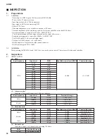
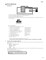
When in the test program execution, select the test program number for the gain encoder and the program can be executed each time
the [+48V] key is pressed.
During selection, the number will flash on the 7segLED and will change to steady on when the program is completed.
The following is the list.
[d00]
Automatic inspection
[d01]
LED inspection
[d02]
SWITCH inspection
[d03] to [d07] is reserve.
[d08] displays the program version. (There is no need to execute during inspection.)
[d09]
Initializes memory
[d10]
System reset
3.
[d00] Automatic inspection
Select the test program number [d00] with the gain encoder. The inspection will be automatically executed when the [+48V] key is
pressed. Or, it can also be executed by entering
<Inspection items (test)>
1. SRAM
CPU connection check
2. SLOT
CPU connection check
3. SLOT clock relationship connection check
4. SLOT power supply peripheral check
5. COM RS422 terminals/ CN903 connection check
6. WORD CLOCK IN/OUT terminal connection check
During the program execution, [d-] will appear on the 7segLED.
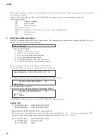
The condition will also appear on the terminal software as shown below.
If the inspection ends normally, the following will appear on the terminal software.
[d00] will also come on 7segLED.
If there is an error, the error list will appear on the terminal software
After [E003] has flashed three times on the 7segLED, [d00] will be displayed steadily.
[ERROR LIST]
[1] SRAM DATA BUS
XXXX XXXX XXXX XXXX
SRAM ADDR BUS
XXXX XXXX XXXX XXX
Results of SRAM (IC923, IC924) and CPU connection check
The first line on the screen shows the condition at the address bus from the left A15, A14 . . . A2, A1 (as viewed from the CPU)
The second line on the screen shows the condition at the data bus from the left D15, D14. . . . D1, D0.
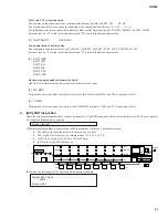
[2] SLOT DATA BUS
XXXX XXXX XXXX XXXX
SLOT ADDR BUS
XXX XXXX XXX
SLOT CONTROL
XXXX
AD824_DIAG>d00
DIAG[00] AUTO CHECK RESULT
OK
AD824_DIAG>
Check SRAM DATA
OOOO OOOO OOOO OOOO OK
Check SRAM ADDR
OOOO OOOO OOOO OOO
OK
:
:
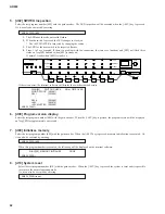
DIAG[00] AUTOCHECK RESULT
NG
ERROR LIST
[6]
COM B
Summary of Contents for AD824
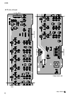
Page 22: ...MAIN Circuit Board B B 3NA V579130 AD824 22 ...
Page 23: ...E B B MAIN MYSL 3NA V579130 MYSL Circuit Board AD824 23 Pattern side Pattern side ...
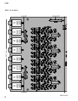
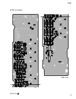
Page 24: ...3NA V579110 INPUT BAL 1 2 3 4 5 6 7 8 1 HA Circuit Board C C AD824 24 ...
Page 25: ...AD824 25 3NA V579110 to MAIN CN903 1 C C to JK CN202 to JK CN102 to DC CN007 Component side ...
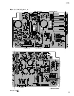
Page 26: ...HA Circuit Board 3NA V579110 1 D D AD824 26 ...
Page 27: ...3NA V579110 1 D D AD824 27 Pattern side ...
Page 30: ...AD824 30 AD Circuit Board 3NA V579120 F F ...
Page 31: ...AD824 31 JK Circuit Board F F AD JK 3NA V579120 Pattern side Pattern side ...
Page 33: ...PN Circuit Board 3NA V579100 1 H H H H AD824 33 Pattern side ...

