AD824
42
5.
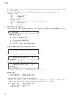
[d02] SWITCH inspection
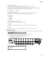
Select the test program number [d02] with the gain encoder. The LED inspection will be executed when the [+48V] key is pressed.
Or, it can also be executed by entering
1. The LED near the relevant switch flashes.
2. When the switch is pressed, the LED changes to steady on.
* The +48V MASTER is inspected by changing the switch.
3. The LED for the next switch to be inspected flashes.
4. Steps 1 to 3 are repeated. If there is a problem with the connection, the time over functions and [E02] will flash three
times on 7segLED and ends when [d02] is steady on.
If normal, it ends when [d02] is steady on.
If there is an error, the terminal software will display the switches that had errors.
6.
[d08] Program version display.
Select the test program number [d08] with the gain encoder. When the [+48V] key is pressed, the program version will be displayed
on 7segLED for approximately one second.
7.
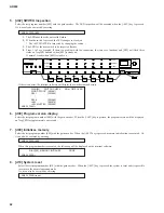
[d09] Initializes memory
Select the test program number [d09] with the gain encoder. When the [+48V] key is pressed, memory initialization is executed. Or,
it can also be executed by entering
When this program number is executed, the following will be displayed on the terminal software.
8.
[d10] System reset
Select the test program number [d10] with the gain encoder. When the [+48V] key is pressed, the system is reset and it is possible
to return to the normal operating mode.
Or, it can also be executed by entering
AD824_DIAG>d02
AD824_DIAG>d09
+48V MASTER
PEAK
NOMINAL
SIGNAL
+48V
PEAK
NOMINAL
SIGNAL
+48V
GAIN
dB
44.1kHz 48kHz
BNC
SLOT
INTERNAL
WORD CLOCK
SEL
1
2
3
4
5
6
7
8
SEL
OFF
ON
DIAG[02]
SWITCH CHECK
NG or TIME OVER
WORD CLOCK (SW961)
SEL 1
(SW962)
:
:
SEL 8
(SW969)
+48V
(SW970)
+48V MASTER
(SW960)
AD824_DIAG>
DIAG[09] MEMORY INITIALIZE
DONE
AD824_DIAG>
AD824_DIAG>reset
Summary of Contents for AD824
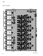
Page 22: ...MAIN Circuit Board B B 3NA V579130 AD824 22 ...
Page 23: ...E B B MAIN MYSL 3NA V579130 MYSL Circuit Board AD824 23 Pattern side Pattern side ...
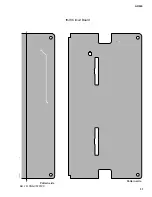
Page 24: ...3NA V579110 INPUT BAL 1 2 3 4 5 6 7 8 1 HA Circuit Board C C AD824 24 ...
Page 25: ...AD824 25 3NA V579110 to MAIN CN903 1 C C to JK CN202 to JK CN102 to DC CN007 Component side ...
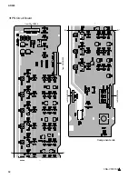
Page 26: ...HA Circuit Board 3NA V579110 1 D D AD824 26 ...
Page 27: ...3NA V579110 1 D D AD824 27 Pattern side ...
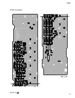
Page 30: ...AD824 30 AD Circuit Board 3NA V579120 F F ...
Page 31: ...AD824 31 JK Circuit Board F F AD JK 3NA V579120 Pattern side Pattern side ...
Page 33: ...PN Circuit Board 3NA V579100 1 H H H H AD824 33 Pattern side ...

