background image

XVME-500/590  Manual
February, 1988

Appendix A

INSTALLING  AN XVME-910 CHANNEL EXPANSION KIT

.

(Optional)

A.1 

INSTALLATION

The number of analog inputs on the  XVME-500/590 can be expanded from 16  single-
ended/8 differential to 32 single-ended/l6 differential by installing an XVME-910
Channel Expansion Kit.

The kit consists of two additional 8 input analog  multi-

plexers. Installation is simply a matter of positioning the two integrated circuits on

the board in locations  U19  and U23, and soldering them in place (see Appendix C,
the assembly drawing for the locations of these  IC’s).

NOTE

Static precautions should be taken when handling the

chips, and a low-wattage soldering iron (30 watts or
less) should be used.

Care should be taken to make sure pin 1 on the chip
is aligned correctly.

A-l

Summary of Contents for XVME 500

Page 1: ......

Page 2: ......

Page 3: ......

Page 4: ......

Page 5: ......

Page 6: ......

Page 7: ...2 programmable gain amp with 25uSec conversion 3 XVME 500 3 and XVME 590 3 programmable gain amp with 10uSec conversion See Table l l Section 1 3 for additional information on conversion time settlin...

Page 8: ...10 channel expansion kit backplane signal pin descriptions block diagram assembly illustration and schematics and a quick reference section 1 3 MODULE OPERATIONAL DESCRIPTION Figure l 1 shows the ope...

Page 9: ......

Page 10: ......

Page 11: ...up to 16 SE or 8 DI signals to be connected to the ADC expansion kit allows double signal input directed by software to select one channel for data conversion Resistor programmable gain with addition...

Page 12: ...selectable programmable gains see Section 2 6 4 l Range 1 xl x2 x5 and x10 Range 2 x4 x8 x20 and x40 Range 3 x10 x20 x50 and x100 A 32 element RAM buffer is provided with the programmable amps to hold...

Page 13: ...Typical 1 90 A 1 60 A Accuracy Resolution Linearity Differential Linearity Monotonicity 12 bits 0 5 LSB 50 5 LSB Guaranteed System Accuracy Gain 1 Gain 10 Gain 100 0 0l FSR max 0 l FSR max 01 FSR max...

Page 14: ...ias Current Input Capacitance Operating Common Mode Voltage Speed Conversion Time versions 1 2 version 3 Throughput Frequency version 1 version 2 version 3 Settling Time version 1 versions 2 3 1 2 5 o...

Page 15: ...30g peak acceleration 11 mSec duration Non operating 50g peak acceleration 11 mSec duration Vibration Operating 5 to 2000Hz 015 in peak to peak 2 5g max Non operating 5 to 2OOOHz 030 in peak to peak 5...

Page 16: ...address locations for analog input are identical 0 All bit definitions for registers are the same EXCEPT there are no LEDs Channel register counter now reset the 540 powers up random receives reset so...

Page 17: ...A A host processor installed in the same backplane A properly installed controller subsystem An example of such a subsystem is the XYCOM XVME 010 System Resource Module B A host processor which incorp...

Page 18: ......

Page 19: ......

Page 20: ......

Page 21: ......

Page 22: ...y interrupts generated by the module See Section 2 5 3 Module base address select jumpers Section 2 5 1 refer to This jumper allows module to respond to supervisory access only when installed or to bo...

Page 23: ...times for the appropriate module amplifier see Section 3 4 1 These two jumpers are provided to allow grounding of an input channel in either the single ended or the differential input mode of operatio...

Page 24: ...ow each jumper relates to the address lines A15 A l 4 A l 3 A l 2 A l l co A10 l Figure 2 3 Base Address Jumpers When a jumper is INSTALLED the corresponding base address bit will be logic 0 However w...

Page 25: ......

Page 26: ...input module can be programmed to generate an interrupt at the completion of a conversion These jumpers determine the level of that interrupt Interrupt level jumper options are defined in Table 2 4 In...

Page 27: ...rol the data formats for the two different voltage modes Table 2 5 Input Conversion Format Jumpers Digital Data Conversion Jumpers Input Format All Inputs Installed Mode Analog to Straight Binary JlA...

Page 28: ...les as follows SE and PDI increase to 32 DI increases to 16 Table 2 6 Single Ended Differential Pseudo Differential Jumper Options Jumpers Set J21A J21C J25 Input Mode Set in this manner the module in...

Page 29: ...GE SELECTION 2 6 4 1 Programmable Gain Selection XVME 500 590 2 XVME 500 590 3 J15 J19 J14 J18 J16 J20 The gain for each input channel is individually programmable over any one of three possible gain...

Page 30: ...selected range 2 6 4 2 Fixed Gains Jumper Selectable version 1 only J6 J7 J8 or J9 The fixed gain for each analog input channel in the version 1 of the XVME 500 590 is selected by installing or removi...

Page 31: ...n increases the versatility of the XVME 500 590 l In order to utilize these gains it is necessary to install 1 A fixed value resistor value determined by equation following 2 A potentiometer for fine...

Page 32: ......

Page 33: ......

Page 34: ...is 6 1K 6100 R13 must be adjusted from 1K to 614K 614 to achieve the desired value NOTE The resistor used should be type RN 55E with a temperature coefficient of 25 ppm Degree C max 6 The resistor RI0...

Page 35: ...d by software Table 2 10 shows the conversion resolution jumpers Table 2 10 Conversion Resolution Jumpers I Conversion Desired Jumper Installed I 1 12 bit J2A 8 bit J2B Figure 2 5 shows the various fo...

Page 36: ...operation inserting jumper J23 shorts input channel 8 to ground Inserting J24 shorts channel 0 to ground In differential mode inserting both J23 channel 0 Hi and J24 channel 0 Lo will short channel 0...

Page 37: ...CH 24 ANALOG GND CH 25 CH 17 ANALOG GND CH 18 CH 26 ANALOG GND CH 27 CH 19 ANALOG GND CH 20 CH 28 Those channels marked by are only available expansion kit is installed Table continued next page Diffe...

Page 38: ...he board see Figure 2 1 or Figure 2 2 The pin connections for Pl a 96 pin 3 row connector contains the standard address data and control signals necessary for the operation of VMEbus defined NEXP modu...

Page 39: ...19 ANALOG GND CH 20 CH 28 ANALOG GND CH 29 CH 21 ANALOG GND CH 22 CH 30 ANALOG GND Differential Configuration P2 Connector CH 0 LO Cl CH 0 HI Al ANALOG GND C 2 CH 1 HI A2 CH 1 LO C 3 ANALOG GND A3 CH...

Page 40: ...alog to binary conversion with J1A Analog to two s complement conversion with J1B Unipolar voltage range selector Bipolar voltage range selector Fixed gain selector x1000 Resistor programmable gain se...

Page 41: ...le base address select jumper Module base address select jumper Module base address select jumper Module base address select jumper Module base address select jumper Module base address select jumper...

Page 42: ...etermine and verify all relevant jumper configurations and all connections to external devices or power supplies Please check the jumper configuration against the diagrams and lists in this manual To...

Page 43: ...lation procedure 1 Turn power off 2 Disconnect the module from the bus 3 Remove the screw and plastic collar assemblies labeled 6 7 from the extreme top and bottom of the existing 3U front panel 11 4...

Page 44: ......

Page 45: ...I O Address Space When the module is installed in a system it will occupy a IK byte block of the Short I O Address Space The base address decoding scheme for the XVME I O modules positions the startin...

Page 46: ...Base OOH 0lH 7EH 80H 82H 84H 86H U N D E F I N E D w w m s w Status Control Reg Interrupter Vector Reg w i Gain Channel Reg A D High Byte A D Low Byte U N D E F I N E D 7FH 81H 83H 85H 87H rlgure 3 l...

Page 47: ...chapter s remaining sections Status Control Register base 81H Section 3 3 1 The status control register contains eight single bit locations which provide control signals to reset the module enable int...

Page 48: ...s control bits Table 3 1 Status Control Register 3 3 1 1 Bit No Function I Status Control 0 1 2 Interrupt Pending No Connection 3 Interrupt Enable Interrupt Enable 4 Board Reset Board Reset 5 Mode 0 M...

Page 49: ...onnector JKl see Figure 3 6 for timing The use of input conversion modes is explained in greater detail in Section 3 4 1 D4 This bit provides a means for a module software reset If toggled to logic l...

Page 50: ...e XVME 500 590 l as displayed in Sections 2 6 4 2 and 2 6 4 3 realizes gains in one of two non software methods The first method is gain selection via jumpers This method allows the input channels to...

Page 51: ...in Channel register is arranged XVME 50012 50013 I XVME 500 l D7 D6 05 04 03 02 Dl D O Selects Gain 00 Gain 1 01 Gain 2 10 Gain 3 11 Gain 4 I Selects Channel I Configures the Register to Program Iogic...

Page 52: ...I 0 0 1 1 D O 0 Channel 0 1 Channel 1 0 Channel 2 1 Channel 3 0 Channel 4 1 Channel 5 0 Channel 6 1 Channel 7 0 Channel 8 1 Channel 9 0 Channel 10 1 Channel 1I 0 Channel 12 1 Channel 13 0 Channel 14 1...

Page 53: ...he register to be used to program initialize gain RAM or it allows the register to be used to read the gain RAM The specific channel can be programmed to apply the chosen gain factor any time it conve...

Page 54: ...dition a conversion is initiated on channel 15 See Figure 3 4 07 06 05 04 03 02 01 DO X X 0 0 1 1 1 1 1 I Gain Factor Enables Selects Channel is read here Register for 15 for a gain Convert Mode Read...

Page 55: ...e Low Byte D15 D14 D13 D12 Dll Dl0 D9 D8 D7 D6 D5 D4 D3 D2 Dl D O Base 86H Base 87H Figure 3 5 A D Data Input Register Format The manner in which data appears at the A D Data Register depends upon whi...

Page 56: ......

Page 57: ......

Page 58: ...2 Jumpers must be configured for the desired interrupt level input type DI or SE and bipolar or unipolar input voltage range input gain range and input binary data format straight binary offset binar...

Page 59: ...ived on Pin 50 ground reference on Pin 49 of connector JKI Four conditions may cause a conversion to be initiated These conditions are 1 Writing to the channel gain register in random channel mode wit...

Page 60: ...base objective is to set both D5 and D6 to logic 0 Select the desired channel by writing the channel number to bits D0 thru D4 of the gain channel register base 85H Assuming the cor responding Gain RA...

Page 61: ...register that sets bit D7 to logic 1 This action will force a conversion on the specified starting channel without incrementing the channel number Then by reading the low order A D data byte base 87H...

Page 62: ...power up this action will initiate a conversion with the correct gain on a specified channel A conversion may also be forced by using bit D7 of the status control register 3 The result of the conversi...

Page 63: ...elect the desired channel by writing the channel number to bits D0 thru D4 of the gain channel register Assuming that the Gain RAM was properly initialized programmed after power up it will not be nec...

Page 64: ...enable the module IACK handling circuitry see Section 2 5 3 2 The Interrupt Vector Register location base 83H must be loaded with the required vector This vector register will be read by the interrupt...

Page 65: ...0 Manual February 1988 The resistors should be 0 l tolerance or better with stable temperature coefficient characteristics e g 25ppm or better All input channels operate with the same full scale input...

Page 66: ...ME 500 or Figure 2 2 XVME 590 Table 4 1 A D Calibration Potentiometers Resistor R2 R8 R9 R17 Rll R13 Description ADC unipolar offset adjust ADC bipolar offset adjust ADC gain adjust Input offset adjus...

Page 67: ...V at TP2 TPl is ground 5 Set the input stage gain to 10 by setting bits D6 and D7 of the Gain Channel register to logic 1 Measure and record the output voltage V at TP2 6 Calculate the voltage offset...

Page 68: ......

Page 69: ......

Page 70: ......

Page 71: ...nsion Kit The kit consists of two additional 8 input analog multi plexers Installation is simply a matter of positioning the two integrated circuits on the board in locations U19 and U23 and soldering...

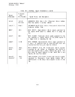
Page 72: ...IA 21 1A 22 1A 23 lB 16 17 18 19 lC 14 lA 18 Signal Name and Description AC FAILURE Open collectors driven signal which indicates that the AC input to the power supply is no longer being provided or t...

Page 73: ...cate that it is using the bus BUS CLEAR Totem pole driven signal generated by the bus arbitrator to request release by the DTB master if a higher level is requesting the bus BUS ERROR Open collector d...

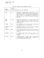
Page 74: ...driven signal that indicates during byte and word transfers that a data transfer will occur on data buss lines D00 D07 DATA STROBE 1 Three state driven signal that indicates during byte and word tran...

Page 75: ...ain INTERRUPT REQUEST l 7 Open collector driven signals generated by an interrupter which carry prioritized interrupt requests Level seven is the highest priority LONGWORD Three state driven signal in...

Page 76: ...ctor driven signal which when low will cause the system to be reset WRITE lA 14 WRITE Three state driven signal that specifies the data transfer cycle in progress to be either read or written A high l...

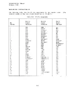
Page 77: ...w A Row B Signal Signal Mnemonic Mnemonic D00 BBSY DO1 BCLR DO2 ACFAIL DO3 BG0IN DO4 BGOOUT DO5 BGlIN DO6 BGlOUT DO7 BG2IN GND BG20UT SYSCLK BG3IN GND BG30UT DSl BRO DSO BRl WRITE BR2 GND BR3 DTACK AM...

Page 78: ...12 PA6 1 P2A 13 PA401 P2B 13 v c c P2C 13 GND P2A 14 PA20I NO CONNECT P2C 14 PA3 1 P2A 15 PA1 1 NO CONNECT P2C 15 GND P2A 16 GND NO CONNECT P2C 16 PAO 1 P2A 17 H4 OUT 2 NO CONNECT P2C 17 G N D P2A 18...

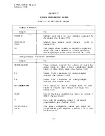
Page 79: ...J8 J9 J7 J14 J15 J16 J18 J19 520 Use These jumpers provide the option of converting analog inputs to either a two s complement straight binary or offset binary format See Section 2 6 1 Selects 12 bit...

Page 80: ...d as either 8 differential 16 single ended or 16 pseudo differential input channels Section 2 6 2 J22A J22B J22C J22D J23 J24 Each jumper is used to determine settling times for the appropriate module...

Page 81: ......

Page 82: ...CH 4 HI 15 ANALOG GND ANALOG GND 16 CH 13 CH 5 HI 17 CH 5 CH 5 LO 18 ANALOG GND ANALOG GND 19 CH 6 CH 6 LO 20 CH 14 CH 6 HI 21 ANALOG GND ANALOG GND 22 CH 15 CH 7 HI 23 CH 7 CH 7 LO 24 ANALOG GND ANA...

Page 83: ...ANALOG GND 40 CH 29 CH 13 HI 41 CH 21 CH 13 LO 42 ANALOG GND ANALOG GND 43 CH 22 CH 14 LO 44 CH 30 CH 14 HI 45 ANALOG GND ANALOG GND 46 CH 31 CH 15 HI 47 CH 23 CH 15 LO 48 ANALOG GND ANALOG GND 49 PO...

Page 84: ...ANALOG GND CH 20 CH 28 ANALOG GND CH 29 CH 21 ANALOG GND CH 22 CH 30 ANALOG GND Differential Configuration P2 Connector CH 0 LO Cl CH 0 HI Al ANALOG GND C 2 CH 1 HI A2 CH 1 LO C 3 ANALOG GND A3 CH 2...

Page 85: ...range selector Fixed gain selector x1000 Resistor programmable gain selector Fixed gain selector x100 Fixed gain selector x10 A3 interrupt level selector A2 interrupt level selector Al interrupt level...

Page 86: ......

Page 87: ...e I A D Low Byte 87H U N D E F I N E D Figure C 2 XVME 500 590 Analog Input Module Memory Map Table C 6 A D Calibration Potentiometers Resistor R2 R8 R9 R17 Rll R13 Description ADC unipolar offset adj...

Page 88: ......

Page 89: ......

Page 90: ......

Page 91: ......

Page 92: ......

Page 93: ......

Page 94: ......

Page 95: ......

Page 96: ......

Page 97: ......

Page 98: ......

Page 99: ......

Page 100: ......

Page 101: ......

Page 102: ......

Reviews: