XVME-500/590 Manual
February, 1988
Chapter 3
PROGRAMMING
3.1 INTRODUCTION
This chapter provides information required to program the XVME-500/590 Analog
Input Module for analog-to-digital signal conversions.
The presentation of the
information is as follows:
l
Presentation of the module address map with programming locations
l
Discussion of base addressing and how the conversion registers are
accessed
A/D conversion modes and principals
3.2 BASE ADDRESSING
The XVME-500/590 Analog Input Module is designed to be addressed within the
VMEbus- defined 64K Short I/O Address Space.
When the module is installed in a
system, it will occupy a IK byte block of the Short I/O Address Space.
The base
address decoding scheme for the XVME I/O modules positions the starting address
for each board on a 1K boundary.
Thus, there are 64 possible base addresses (1K
boundaries) for the XVME-500/590 within the Short I/O Address Space. (Refer to
Section 2.5.1 for the list of base addresses and their corresponding list of jumper
c o n f i g u r a t i o n s . )
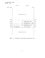
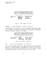
The logical registers utilized for the conversion data on the XVME-500/590 are
given specific addresses within the 1K of block-address space occupied by the
module. These addresses are offset from the module base address. Figure 3-1
shows a representative memory map for the XVME-500/590 module.
3-l
Summary of Contents for XVME 500
Page 1: ......
Page 2: ......
Page 3: ......
Page 4: ......
Page 5: ......
Page 6: ......
Page 9: ......
Page 10: ......
Page 18: ......
Page 19: ......
Page 20: ......
Page 21: ......
Page 25: ......
Page 32: ......
Page 33: ......
Page 44: ......
Page 56: ......
Page 57: ......
Page 68: ......
Page 69: ......
Page 70: ......
Page 81: ......
Page 86: ......
Page 88: ......
Page 89: ......
Page 90: ......
Page 91: ......
Page 92: ......
Page 93: ......
Page 94: ......
Page 95: ......
Page 96: ......
Page 97: ......
Page 98: ......
Page 99: ......
Page 100: ......
Page 101: ......
Page 102: ......

