background image

44

www.xilinx.com

SP605 Hardware User Guide

UG526 (v1.1.1) February 1, 2010

Chapter 1:

SP605 Evaluation Board

User SIP Header

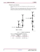
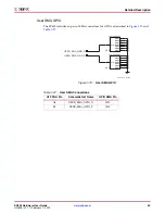
The SP605 includes a 6-pin single-inline (SIP) male pin header (J55) for FPGA GPIO access. 
Four pins of J55 are wired to the FPGA through 200 ohm series resistors and a level shifter, 
and the remaining two J55 pins are wired to 3.3V and GND. The J55 header is described in 

Figure 1-18

 and 

Table 1-26

.

Note:

This header is not installed on the SP605 as built.

X-Ref Target - Figure 1-1

8

Figure 1-18:

User SIP Header J55

VCC3V3

HDR_1x6

GPIO_HEADER_3

GPIO_HEADER_2

GPIO_HEADER_1

GPIO_HEADER_0

2

1

5%

1/16W

200

R281

1

2

R280

200

1/16W

5%

1

2

3

4

5

6

J55

DNP

1

2

R282

200

1/16W

5%

2

1

5%

1/16W

200

R283

TXB0108

VCCB

B1
B2
B3
B4

B6
B7

GND

A3

A8
OE

A4
A5

A7

A6

B5

A1
A2

B8

VCCA

VCC1V5_FPGA

VCC3V3

GPIO_HEADER_0
GPIO_HEADER_1
GPIO_HEADER_2
GPIO_HEADER_3

GPIO_HEADER_0_L

S

GPIO_HEADER_1_L

S

NC

NC
NC
NC

2

12

3

1

15

7
8

6

5

10

9

4

11

13

14

16

17

18

20

19

U52

1

2

X5R

10V

0.1UF

C385

2

1

C384

0.1UF

10V

X5R

NC

NC

NC

NC

GPIO_HEADER_2_L

S

GPIO_HEADER_3_L

S

U1 FPGA Pin

G7

H6
D1

R7

 UG526_18 _092409

Table 1-26:

User SIP Header Connections

U1 FPGA Pin

Schematic Net Name

GPIO Header Pin

G7

GPIO_HEADER_0

J55.1

H6

GPIO_HEADER_1

J55.2

D1

GPIO_HEADER_2

J55.3

R7

GPIO_HEADER_3

J55.4


GND

J55.5

 –

VCC3V3

J55.6

Notes: 

1. Each GPIO_HEADER_

n

 signal is sourced from the FPGA as 

<

netname

>_LS to a level shifter, then to the J55 header.

2. Each GPIO_HEADER_n net has a 200 ohm series resistor between 

the level shifter and its respective header pin.

Summary of Contents for SP605

Page 1: ...Guide Subtitle optional UG526 v1 1 1 February 1 2010 optional SP605 Hardware User Guide UG526 v1 1 1 February 1 2010...

Page 2: ...you in connection with the Information THE DOCUMENTATION IS DISCLOSED TO YOU AS IS WITH NO WARRANTY OF ANY KIND XILINX MAKES NO OTHER WARRANTIES WHETHER EXPRESS IMPLIED OR STATUTORY REGARDING THE DOC...

Page 3: ...m ACE CF and CompactFlash Connector 20 6 USB JTAG 22 7 Clock Generation 23 Oscillator Differential 23 Oscillator Socket Single Ended 2 5V or 3 3V 24 SMA Connectors Differential 25 8 Multi Gigabit Tran...

Page 4: ...gh 48 Mode DIP Switch SW1 Active High 49 18 VITA 57 1 FMC LPC Connector 50 Power Management 52 AC Adapter and 12V Input Power Jack Switch 52 Onboard Power Regulation 53 Configuration Options 55 Append...

Page 5: ...verview This overview outlines the features and product selection of the Spartan 6 family Spartan 6 FPGA Data Sheet DC and Switching Characteristics This data sheet contains the DC and switching chara...

Page 6: ...of the DSP48A1 slice in Spartan 6 FPGAs and provides configuration examples Spartan 6 FPGA Memory Controller User Guide This guide describes the Spartan 6 FPGA memory controller block a dedicated emb...

Page 7: ...itional information and support material is located at http www xilinx com sp605 This information includes Current version of this user guide in PDF format Example design files for demonstration of Sp...

Page 8: ...2 5V 27MHz oscillator single ended SMA connectors differential SMA connectors for MGT clocking differential 8 Multi Gigabit Transceivers GTP MGTs FMC LPC connector SMA PCIe SFP module connector 9 PCI...

Page 9: ...SP605 and its peripherals X Ref Target Figure 1 1 Figure 1 1 SP605 Features and Banking Spartan 6 XC6SLX45T 3FGG484 U1 PCIe 125 MHz Clk SMA REFCLK SFPCLK FMC GBTCLK Bank 0 2 5V Bank 1 2 5V Bank 3 1 5V...

Page 10: ...gure 1 2 shows a board photo with numbered features corresponding to Table 1 1 and the section headings in this document The numbered features in Figure 1 2 correlate to the features and notes listed...

Page 11: ...MA 13 9 PCIe 1 lane edge conn Gen 1 Card Edge Connector 1 lane 12 10 SFP Module Cage Connector AMP 136073 1 12 11 Ethernet 10 100 1000 Marvell M88E1111 EPHY 11 12 USB UART USB to UART Bridge Silicon L...

Page 12: ...nfiguring the FPGA see Configuration Options Mode switch SW1 see Table 1 30 page 55 is set to 10 Slave SelectMAP to choose the System ACE CF default configuration References See the Spartan 6 FPGA Con...

Page 13: ...The Spartan 6 FPGA hard memory controller is used for data transfer across the DDR3 memory interface s 16 bit data path using SSTL15 signaling The maximum data rate supported is 800 Mb s with a memory...

Page 14: ...Connections U1 FPGA Pin Schematic Net Name Memory U42 Pin Number Pin Name K2 MEM1_A0 N3 A0 K1 MEM1_A1 P7 A1 K5 MEM1_A2 P3 A2 M6 MEM1_A3 N2 A3 H3 MEM1_A4 P8 A4 M3 MEM1_A5 P2 A5 L4 MEM1_A6 R8 A6 K6 MEM...

Page 15: ...3 MEM1_DQ12 A3 DQ15 W1 MEM1_DQ13 C8 DQ10 Y2 MEM1_DQ14 B8 DQ14 Y1 MEM1_DQ15 A7 DQ12 H2 MEM1_WE_B L3 WE_B M5 MEM1_RAS_B J3 RAS_B M4 MEM1_CAS_B K3 CAS_B L6 MEM1_ODT K1 ODT K4 MEM1_CLK_P J7 CLK_P K3 MEM1_...

Page 16: ...Winbond W25Q64VSFIG 64 Mb flash memory device U32 and a flash programming header J17 J17 supports a user defined SPI mezzanine board The SPI configuration source is selected via SPI select jumper J46...

Page 17: ...et for more information Ref 4 Table 1 6 SPI x4 Memory Connections U1 FPGA Pin Schematic Net Name SPI MEM U32 SPI HDR J17 Pin Pin Name Pin Pin Name AB2 FPGA_PROG_B 1 T14 FPGA_D2_MISO3 1 IO3_HOLD_B 2 R1...

Page 18: ...Configuration Options X Ref Target Figure 1 5 Figure 1 5 Linear BPI Flash Interface Table 1 7 Linear Flash Connections U1 FPGA Pin Schematic Net Name U25 BPI FLASH Pin Number Pin Name N22 FLASH_A0 29...

Page 19: ...9 DQ2 AA6 FLASH_D3 41 DQ3 AB6 FLASH_D4 47 DQ4 Y5 FLASH_D5 49 DQ5 AB5 FLASH_D6 51 DQ6 W9 FLASH_D7 53 DQ7 T7 FLASH_D8 35 DQ8 U6 FLASH_D9 37 DQ9 AB19 FLASH_D10 40 DQ10 AA18 FLASH_D11 42 DQ11 AB18 FLASH_D...

Page 20: ...System ACE CF controller supports up to eight configuration images on a single CompactFlash card The configuration address switches allow the user to choose which of the eight configuration images to...

Page 21: ...Compact Flash CF card is installed in the CF socket U37 the System ACE CF will attempt to load a bitstream from the CF card image address pointed to by the image select switch S1 Every time a Compact...

Page 22: ...takes priority over the mode pin settings AA1 SYSACE_MPBRDY 39 MPBRDY W4 SYSACE_MPCE 42 MPCE AA2 SYSACE_MPIRQ 41 MPIRQ T6 SYSACE_MPOE 77 MPOE T5 SYSACE_MPWE 76 MPWE G17 SYSACE_CFGTDI 81 CFGTDI A21 FP...

Page 23: ...FPGA The iMPACT software tool can also program the BPI flash via the USB J4 connection iMPACT can download a temporary design to the FPGA through the JTAG This provides a connection within the FPGA fr...

Page 24: ...oscillator installed Figure 1 8 shows the unpopulated user oscillator socket This figure indicates the socket pin 1 location Figure 1 9 shows the oscillator installed with its pin 1 location identifi...

Page 25: ...oint P4 edge connector fingers One 1 MGT is wired to the FMC LPC connector J2 One 1 MGT is wired to MGT SMA connectors J36 J37 One 1 MGT is wired to the SFP Module connector P4 The SP605 includes a se...

Page 26: ...ND2 GND3 GND4 GND5 GND6 GND7 SIG GND1 GND2 GND3 GND4 GND5 GND6 GND7 SIG SMA MGT Connectors MGT REFCLK 2 3 4 5 6 7 8 1 J35 32K10K 400E3 2 3 4 5 6 7 8 1 32K10K 400E3 J34 1 8 7 6 5 4 3 2 32K10K 400E3 J36...

Page 27: ...UG526 v1 1 1 February 1 2010 Detailed Description Table 1 10 GTP SMA Clock Connections U1 FPGA Pin Schematic Net Name SMA Pin C9 SMA_RX_N J35 1 D9 SMA_RX_P J34 1 A8 SMA_TX_N J33 1 B8 SMA_TX_P J32 1 D1...

Page 28: ...its load regulation should be better than 10 SP605 power slide switch SW2 turns the board on and off by controlling the 12V supply to the board Caution Caution Never apply power to the power brick 6 p...

Page 29: ...f 6 Also see the following websites for more information about the Spartan 6 FPGA Integrated Endpoint Block for PCI Express Product information http www xilinx com products ipcenter S6_PCI_Express_Blo...

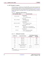
Page 30: ...e Control and Status SFP Control Status Signal Board Connection SFP_TX_FAULT Test Point J15 High Fault Low Normal Operation SFP_TX_DISABLE Jumper J44 Off SFP Enabled On SFP Disabled SFP_MOD_DETECT Tes...

Page 31: ...ws the connections and pin numbers for the PHY Table 1 14 PHY Configuration Pins Pin Connection on Board Bit 2 Definition and Value Bit 1 Definition and Value Bit 0 Definition and Value CFG2 VCC 2 5V...

Page 32: ...P Tri Mode Ethernet MAC User Guide Ref 7 U22 PHY_RXD7 120 RXD7 AB7 PHY_TXC_GTPCLK 14 GTXCLK L20 PHY_TXCLK 10 TXCLK U8 PHY_TXER 13 TXER T8 PHY_TXCTL_TXEN 16 TXEN U10 PHY_TXD0 18 TXD0 T10 PHY_TXD1 19 TX...

Page 33: ...ions with the SP605 Refer to the evaluation kit Getting Started Guide for driver installation instructions References Refer to the Silicon Labs website for technical information on the CP2103GM and th...

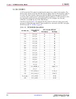
Page 34: ...7301C is controlled by way of the video IIC bus The DVI connector Table 1 18 supports the IIC protocol to allow the board to read the monitor s configuration parameters These parameters can be read by...

Page 35: ...tems FPGA U1 Bank 0 SFP IIC interface SFP module connector P2 The SP605 IIC bus topology is shown in Figure 1 11 X Ref Target Figure 1 11 Figure 1 11 IIC Bus Topology U1 P3 U31 BANK 1 IIC_SDA_MAIN IIC...

Page 36: ...J2 C30 U4 6 1 AA4 IIC_SDA_DVI Q8 2 U31 14 Q8 3 P3 7 IIC_SDA_DVI_F W13 IIC_SCL_DVI Q7 2 U31 15 Q7 3 P3 6 IIC_CLK_DVI_F E6 IIC_SDA_SFP P2 4 E5 IIC_SCL_SFP P2 5 Notes 1 U4 IIC bus signals are resistivel...

Page 37: ...Ref 18 In addition see the Xilinx XPS IIC Bus Interface Data Sheet Ref 8 Table 1 20 IIC Memory Connections U1 FPGA Pin Schematic Netname IIC Memory U4 Pin Number Pin Name Not Applicable Tied to GND 1...

Page 38: ...reen GPIO_LED_1 DS5 GPIO_LED_2 Green GPIO_LED_2 DS6 GPIO_LED_3 Green GPIO_LED_3 DS7 FPGA_AWAKE Green FPGA AWAKE DS8 SYSACE_STAT_LED Green System ACE CF Status LED System ACE CF Status DS9 TI_PWRGOOD A...

Page 39: ...them visible on the connector end of the board when the SP605 board is installed into a PC motherboard This cluster of six LEDs is installed adjacent to the RJ45 Ethernet jack P1 X Ref Target Figure...

Page 40: ...LED DS2 comes on after the FPGA programming bitstream has been downloaded and the FPGA successfully configured X Ref Target Figure 1 14 Figure 1 14 FPGA INIT and DONE LEDs Table 1 22 FPGA INIT and DO...

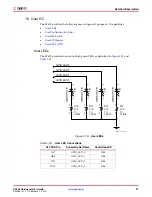
Page 41: ...ur active High green LEDs as described in Figure 1 15 and Table 1 23 X Ref Target Figure 1 15 Figure 1 15 User LEDs Table 1 23 User LED Connections U1 FPGA Pin Schematic Net Name Controlled LED D17 GP...

Page 42: ...6 Four pushbuttons are assigned as GPIO and the fifth is assigned as a CPU_RESET Figure 1 16 and Table 1 24 describe the pushbutton switches X Ref Target Figure 1 16 Figure 1 16 User Pushbutton Switch...

Page 43: ...ulled up to 1 5V when closed X Ref Target Figure 1 17 Figure 1 17 User DIP Switch S2 Table 1 25 User DIP Switch Connections U1 FPGA Pin Schematic Net Name DIP Switch Pin C18 GPIO_SWITCH_0 S2 1 Y6 GPIO...

Page 44: ...DNP 1 2 R282 200 1 16W 5 2 1 5 1 16W 200 R283 TXB0108 VCCB B1 B2 B3 B4 B6 B7 GND A3 A8 OE A4 A5 A7 A6 B5 A1 A2 B8 VCCA VCC1V5_FPGA VCC3V3 GPIO_HEADER_0 GPIO_HEADER_1 GPIO_HEADER_2 GPIO_HEADER_3 GPIO_...

Page 45: ...19 and Table 1 27 X Ref Target Figure 1 19 Figure 1 19 User SMA GPIO Table 1 27 User SMA Connections U1 FPGA Pin Schematic Net Name GPIO SMA Pin A3 USER_SMA_GPIO_N J39 1 B3 USER_SMA_GPIO_P J40 1 GND1...

Page 46: ...e 1 20 Figure 1 20 Power On Off Slide Switch SW2 UG526_20 _100609 N C 12v 12v N C COM COM 1 4 2 3 6 1 2 3 4 5 NC NC 39 30 1060 ATX Peripheral Cable Connector can plug into J27 when SP605 is in PC and...

Page 47: ...on mode pin is high enabled by closing DIP switch S1 switch 4 the System ACE CF controller configures the FPGA from the CompactFlash card when a card is inserted or the SYSACE RESET button is pressed...

Page 48: ...e System ACE CF controller to configure the FPGA from the CompactFlash card when a card is inserted or the SYSACE RESET button is pressed See 5 System ACE CF and CompactFlash Connector page 20 for mor...

Page 49: ...24 and Table 1 30 page 55 References For more information refer to the Spartan 6 FPGA Configuration User Guide Ref 2 See Table 1 30 page 55 for the configuration modes X Ref Target Figure 1 24 Figure...

Page 50: ...400 pins present and the LPC version is partially populated with 160 pins The 10 x 40 rows of a FMC LPC connector provides connectivity for 68 single ended or 34 differential user defined signals 1 MG...

Page 51: ...H10 D14 FMC_LA09_P F7 C15 FMC_LA10_N H11 D15 FMC_LA09_N F8 C18 FMC_LA14_P C17 D17 FMC_LA13_P G16 C19 FMC_LA14_N A17 D18 FMC_LA13_N F17 C22 FMC_LA18_CC_P T12 D20 FMC_LA17_CC_P Y11 C23 FMC_LA18_CC_N U1...

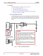
Page 52: ...18 The ATX 6 pin connector has a different pinout than SP605 J18 and connecting the ATX 6 pin connector will damage the SP605 and void the board warranty Caution DO NOT apply power to 6 pin Mini Fit t...

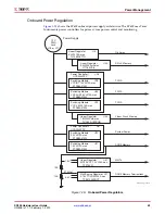
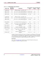
Page 53: ...A max PTD08A010W Linear Regulator U51 MGT AVCC 1 2V 3A max TPS74401 Sink Source Regulator U11 0 75 VTT VREF 3A max TPS51200DRCT Power Controller 1 U26 UCD9240PFC PWR Switching Module U18 Switching Mod...

Page 54: ...PMBus Controller Core Addr 52 21 PTD08A010W U18 10A 0 6V 3 6V Adj Switching Regulator VCCINT_FPGA 1 20V 22 PTD08A010W U19 10A 0 6V 3 6V Adj Switching Regulator VCC2V5_FPGA 2 50V 23 PTD08A010W U20 10A...

Page 55: ...d a bitstream from the CF card image address pointed to by the image select switch S1 With no CF card present the SP605 can be configured via the onboard JTAG controller and USB download cable as desc...

Page 56: ...56 www xilinx com SP605 Hardware User Guide UG526 v1 1 1 February 1 2010 Chapter 1 SP605 Evaluation Board...

Page 57: ...SP605 Table A 1 Default Switch Settings REFDES Function Type Default SW2 Board power slide switch off SW1 FPGA mode 2 pole DIP switch Slave SelectMAP default selects System ACE CF configuration 2 M1 1...

Page 58: ...Table A 2 Default Jumper Settings Jumper REFDES Function Default FMC JTAG Bypass J19 exclude FMC LPC connector J2 Jump 1 2 SFP Module J22 SFP Full BW Jump 1 2 J44 SFP Enabled Jump 1 2 SPI Memory Sele...

Page 59: ...C 15 NC NC GND LA12_P NC NC LA09_N LA10_N NC NC 16 NC NC LA11_P LA12_N NC NC GND GND NC NC 17 NC NC LA11_N GND NC NC LA13_P GND NC NC 18 NC NC GND LA16_P NC NC LA13_N LA14_P NC NC 19 NC NC LA15_P LA16...

Page 60: ...60 www xilinx com SP605 Hardware User Guide UG526 v1 1 1 February 1 2010 Appendix B VITA 57 1 FMC LPC Connector Pinout...

Page 61: ...B LOC L15 13 on U31 NET DVI_V LOC B22 5 on U31 thru series R42 47 5 ohm NET DVI_XCLK_N LOC C22 56 on U31 NET DVI_XCLK_P LOC C20 57 on U31 NET FLASH_A0 LOC N22 29 on U25 NET FLASH_A1 LOC N20 25 on U25...

Page 62: ...2 NET FMC_LA11_N LOC G15 H17 on J2 NET FMC_LA11_P LOC H14 H16 on J2 NET FMC_LA12_N LOC G13 G16 on J2 NET FMC_LA12_P LOC H13 G15 on J2 NET FMC_LA13_N LOC F17 D18 on J2 NET FMC_LA13_P LOC G16 D17 on J2...

Page 63: ...GPIO_HEADER_0 series R283 200 ohm 4 on J55 NET GPIO_LED_0 LOC D17 2 on DS3 LED NET GPIO_LED_1 LOC AB4 2 on DS4 LED NET GPIO_LED_2 LOC D21 2 on DS5 LED NET GPIO_LED_3 LOC W15 2 on DS6 LED NET GPIO_SWI...

Page 64: ...6 NET PHY_TXCLK LOC L20 10 on U46 NET PHY_TXCTL_TXEN LOC T8 16 on U46 NET PHY_TXC_GTXCLK LOC AB7 14 on U46 NET PHY_TXD0 LOC U10 18 on U46 NET PHY_TXD1 LOC T10 19 on U46 NET PHY_TXD2 LOC AB8 20 on U46...

Page 65: ...NET USER_CLOCK LOC AB13 NET USER_SMA_CLOCK_N LOC M19 NET USER_SMA_CLOCK_P LOC M20 NET USER_SMA_GPIO_N LOC A3 NET USER_SMA_GPIO_P LOC B3 Note 1 Pullup and pulldown resistors which branch from nets are...

Page 66: ...66 www xilinx com SP605 Hardware User Guide UG526 v1 1 1 February 1 2010 Appendix C SP605 Master UCF...

Page 67: ...stem ACE CompactFlash Solution Data Sheet 6 UG386 Spartan 6 FPGA GTP Transceivers User Guide 7 UG138 LogiCORE IP Tri Mode Ethernet MAC v4 2 User Guide 8 DS606 XPS IIC Bus Interface Data Sheet 9 UG381...

Reviews: