


ML505/ML506/ML507 Evaluation Platform
www.xilinx.com
25
UG347 (v3.1.1) October 7, 2009
Detailed Description
R
have the IIC pull-up resistors present on the expansion card. Bidirectional level shifting
transistors allow the expansion card to utilize 2.5V to 5V signaling on the IIC bus.
Power supply connections to the expansion connectors provide ground, 2.5V, 3.3V, and 5V
power pins. If the expansion card draws significant power from the ML50
x
board, ensure
that the total power draw can be supplied by the board.
The ML50
x
expansion connector is backward compatible with the expansion connectors
on the ML40
x
, ML32
x
, and ML42
x
boards, thereby allowing their daughter cards to be
used with the ML50
x
Evaluation Platform.
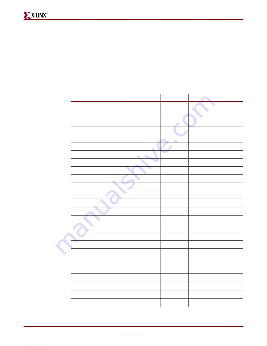
Table 1-11
summarizes the additional
expansion I/O connections.
Table 1-11:
Additional Expansion I/O Connections (J5)
J5 Pin
Label
FPGA Pin
Description
1
VCC5
–
5V Power Supply
2
VCC5
–
5V Power Supply
3
VCC5
–
5V Power Supply
4
VCC5
–
5V Power Supply
5
NC
–
Not Connected
6
VCC3V3
–
3.3V Power Supply
7
VCC3V3
–
3.3V Power Supply
8
VCC3V3
–
3.3V Power Supply
9
VCC3V3
–
3.3V Power Supply
10
NC
–
Not Connected
11
FPGA_EXP_TMS
–
Expansion TMS
12
FPGA_EXP_TCK
–
Expansion TCK
13
FPGA_EXP_TDO
–
Expansion TDO
14
FPGA_EXP_TDI
–
Expansion TDI
15
GPIO_LED_N
AF13
LED North
16
SW3 (N)
U8
GPIO Switch North
17
GPIO_LED_C
E8
LED Center
18
SW14 (C)
AJ6
GPIO Switch Center
19
GPIO_LED_W
AF23
LED West
20
SW13 (W)
AJ7
GPIO Switch West
21
GPIO_LED_S
AG12
LED South
22
SW11 (S)
V8
GPIO Switch South
23
GPIO_LED_E
AG23
LED East
24
SW12 (E)
AK7
GPIO Switch East
25
GPIOLED 0
H18
GPIO LED 0
electronic components distributor


