AMS101 Evaluation Card User Guide
www.xilinx.com
43
UG886 (v1.3) November 6, 2013
XADC Performance Tests
Linearity
Select the
Linearity
tab to perform a linearity test on the XADC. During this test, the signal
source is used as a map source to the XADC.
When the
Collect Data
button is clicked in the GUI, the DAC begins to ramp up and the
XADC results are collected into a histogram. This histogram data is then transferred to the
GUI through the USB-UART connection and a differential non-linearity (DNL) and
integral non-linearity (INL) calculation are performed. This data then displays.
Sensor Data
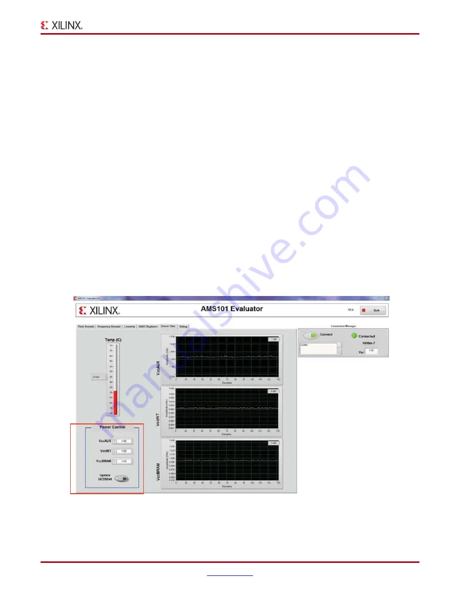
The XADC block contains four integrated sensors within the FPGA. The first is a
temperature sensor and the other three monitor the FPGA voltage supplies: V
CCAUX
,
V
CCINT
, and V
CCBRAM
. These sensors are all digitized by the XADC when the XADC is in
default mode or when they are enabled as part of the channel sequence of the XADC.
When the
Sensor Data
tab is selected, all of the XADC settings are stored in memory in the
GUI. The part is then forced into Default mode. See
7 Series FPGAs and Zynq-7000 All
Programmable SoC XADC Dual 12-Bit 1 MSPS Analog-to-Digital Converter User Guide
(UG480)
[Ref 6]
. The digitized representation for the XADC then displays.
The
Power Control
panel highlighted in
Figure 4-7
can be used to modify physical
voltages being applied to the three supplies in question: V
CCAUX
, V
CCINT
, and V
CCBRAM
.
After changing the voltages and clicking the
Update UCD9248
button, the corresponding
plot should change, showing the actual voltage now being applied to the part within the
part itself.
X-Ref Target - Figure 4-7
Figure 4-7:
Sensor Data Tab and Power Control Panel
UG
88
6_c4_07_11041
3
Ch
a
nge the
a
ct
ua
l volt
a
ge
s
b
eing
a
pplied to the FPGA
with the Tex
as
In
s
tr
u
ment
s
UCD924
8
power controller.


