MODELS 452/452-01 & 852/852-01
SIGNAL PROCESSING FILTERS
FUNCTIONS
Low Pass, High Pass, Band Pass,
Band Reject, Notch (452/452-01
only).
Frequency Range and Resolution
Th ree 11-position switches and one
4-position multiplier (option 01 adds
fifth position to multiplier).
Multiplier
x 1"
x10
x 100
x 1k
x 10k
'Option
01
only.
Frequency
(Hz)
0.01 to 11.1
0.1 to 111
1 to 1.11 k
10 to 11.1 k
100 to 111 k
Resolution
(Hz)
0.01
0.1
1
10
100
Attenuation Rate per channel
452/452-01: 24 dBloctave
852/852-01: 48 dBloctave
FLAT AMPLITUDE (BUTTERWORTH)
RESPONSE
Passband Gain (452/452·0 1)
Low Pass: 0 dB/20 dB,
±
0.25 dB.
High Pass: 0 dB/20 dB,
±
0.25 dB.
(±
0.5 dB in
x
10k Multiplier
position); - 3 dB at approx. 2 MHz.
Passband Gain (852/852·01)
Low Pass: 0 dB/20 dB,
±
0.5 dB.
High Pass: 0 dB/20 dB,
±
0.5 dB
(±
1 dB in
x
10k Multiplier position):
- 3 dB at approx. 1 MHz.
Oj
�
20
L.U
040
:::J
t-
�
60
�
«
80
100
- -
- - - -
. 01 .02 .04.08.1 .2 .4 .81 2 4 810 20 40 80
NORMALIZED FREQUENCY·
fife
Band Reject (1) and Sharp Notch (2) Obtained
by Parallel Connection of 24 dB/Octave Filter
Channels
INPUT STEP
OUTPUT, FLAT
AMPL. POSITION
OUTPUT, FLAT
DELAY POSITION
Transient Response - Low Pass Mode
Attenuation at Cutoff
3 dB.
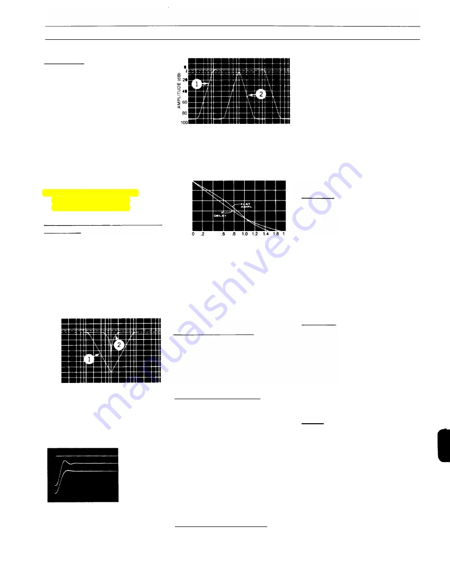
Maximum Stopband Attenuation
90 dB.
,
-
_
,
. ,
.01 .02 .04 .08.1
.
2
.4 .81 2 4 810 20 40
80
NORMALIZED FREQUENCY
(fife)
Band Pass (1) with LP
=
0.01 HP and Minimum
Bandwidth Band Pass (2) with LP
=
HP Obtained by
Series Connection of 4810ctave Filter Channels.
o
_
100
(!l
«
-;' 200
(!l
w
e. 300
w
�
400
I
a. 500
FLA
.4
B
NORMALIZED FREQUENCY
(fife)
Phase Characteristics - Low Pass Mode
Phase Match Between Channels
(Typical)
452/452-01: 1 ° or 1 %, whichever is
greater.
852/852-01: 2° or 2%, whichever is
greater.
FLAT DELAY RESPONSE
Low Pass Delay (Typical)
452/452-01: 1/(2f
c
)
sec.
852/852-01: 1/f
c
sec.
Attenuation Cutoff
452/452-01 : Approx 9 dB.
852/852-01: Approx 17 dB.
INPUT CHARACTERISTICS
Circuit
Single-ended, diode protected.
Impedance
1
M
O
shunted to 50 pF; 75 pF in 20 dB
gain (852/852-01).
Full·Scale Signal at 0 dB Gain
±
10V (7.1 Vrms), DC to 300 kHz,
decreasing to
±
4V (2.8 Vrms) at
1 MHz (divide these by 10 at 20 dB
gain).
Absolute Max Input
±
100 Volts.
Max. DC Component (High Pass)
±
100V, 0 dB gain.
±
10V, 20 dB Gain.
OUTPUT CHARACTERISTICS
Circuits
Single-ended. Short-circuit protected
may be DC isolated from power
ground by rear panel switch.
Impedance
500.
Full·Scale Signal
±
10V (7.1 Vrms), DC to 300 kHz,
decreasing to
±
4V (2.8 Vrms) at
1 MHz (RL �5
kO),
±
15 mA max.
current.
Broadband Noise at Either Gain Setting
( 100 kHz detector bandwidth)
452/452-01: 100 ttVrms.
852/852-01: 200 ttVrms.
Harmonic Components
(Input f
=
1 kHz)
452/452-01: 90 dB below full-scale.
852/852-01: 80 dB below full-scale.
DC Offset at 25°C
452/452-01: 0
±
2.5 mV dc.
852/852-01: 0
±
2.5 mV dc.
GENERAL
Environmental
Operating Temperature: O°C to
+50°C.
Storage Temperature: - 20°C to
+ 70°C .
Dimensions
43.2 cm (17 in.) wide; 8.9 cm (3'/2 in.)
high; 33 cm (13 in.) deep.
Weight
Model 452: 4.5 kg (10 Ib) net.
6.4 kg (14 Ib) shipping.
Model 852: 5.5 kg (12 Ib) net.
6.8 kg (15 Ib) shipping.
Power
115/230V
±
10%, 50 to 500 Hz, 5
watts.
OPTIONS
01: Range Extension
Extends low frequency range and
resolution to 0.01 Hz; performance
specifications remain the same,
except AC line-related spurious com
ponents degraded by 6 dB when
operating in the optional range.
Factory installed .
02: 6000 Output Impedance
04: Rack·Mount Kit
Field-installable.
PRICE (FOB Rockleigh)
Model 452
Model 852
Model 452·01
Model 852·01
Option 02
Option 04
$1700
$2300
$1900
$2650
$50
$25
10
Summary of Contents for 452
Page 16: ......


